Continue to Site

Welcome to EDAboard.com

Welcome to our site! EDAboard.com is an international Electronics Discussion Forum focused on EDA software, circuits, schematics, books, theory, papers, asic, pld, 8051, DSP, Network, RF, Analog Design, PCB, Service Manuals... and a whole lot more! To participate you need to register. Registration is free. Click here to register now.

Working Principle of Bandgap reference ckt

Status
Not open for further replies.

haideruet

Newbie level 4
Joined
Apr 21, 2009
Messages
7
Helped
0
Reputation
0
Reaction score
0
Trophy points
1
Activity points
0
Hi ,
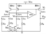
If any body can explain the working principle of this bgr ckt which is attached. or a general bgr ckt.
I am confused whether at the input of the opamp, one input should be PTAT and other be at CTAT?
Ikept the both inputs varying on the same direction with bell shape when we see volt vs Temp. because we have to sum together thats why if same inputs are given to diff.amp. it will again make difference so , ultimatly we get Sum.
Sincere Thanks
HaiderUet
 

Attachments

  • bgr Low Voltage.png
    bgr Low Voltage.png
    32.6 KB · Views: 108

Basically the function of the amplifer is to keep the current so that both amp inputs are equal. The refrence voltage is then replicated over R4.
V+ is the PTAT voltage V- is the CTAT.
IR2=Vbe1/R2, IR3=(VBE1-VBE2)/R3 -> IMP2=Vbe1/R2+DVbe/R3
Assuming MP3=MP2 :IMP2=IMP3
Vbg=R4*(Vbe1/R2+DVbe/R3)=R4/R2*(Vbe1+(R2/R3)*DVbe)
R2/R3 is the factor which you tune the PTAT to cancel the CTAT and to get temperature independent voltage reference.
 
Thanks for your reply ,
Does the size of the PMOS transistors affect the Vbg for adjustments or we can choose any value?
So, you mean the output of the diff amp will be zero if both are inputs are equal and opposite. only the CM level will be seen at output e.g 500m in case of cancellations.
Thanks

Basically the function of the amplifer is to keep the current so that both amp inputs are equal. The refrence voltage is then replicated over R4.
V+ is the PTAT voltage V- is the CTAT.
IR2=Vbe1/R2, IR3=(VBE1-VBE2)/R3 -> IMP2=Vbe1/R2+DVbe/R3
Assuming MP3=MP2 :IMP2=IMP3
Vbg=R4*(Vbe1/R2+DVbe/R3)=R4/R2*(Vbe1+(R2/R3)*DVbe)
R2/R3 is the factor which you tune the PTAT to cancel the CTAT and to get temperature independent voltage reference.
 

Status
Not open for further replies.

Part and Inventory Search

Welcome to EDABoard.com

Sponsor

Back
Top