Continue to Site

Welcome to EDAboard.com

Welcome to our site! EDAboard.com is an international Electronics Discussion Forum focused on EDA software, circuits, schematics, books, theory, papers, asic, pld, 8051, DSP, Network, RF, Analog Design, PCB, Service Manuals... and a whole lot more! To participate you need to register. Registration is free. Click here to register now.

[SOLVED] Feed track and Ground Pour distance for Antenna

Status
Not open for further replies.

Sherry1

Member level 3
Joined
Apr 4, 2013
Messages
61
Helped
0
Reputation
0
Reaction score
0
Trophy points
1,286
Location
Manchester, UK
Activity points
1,810
I am making a feed trace on a FR4 PCB for my antenna. There is a ground pour around it and then VIAs take the Ground plane to a layer below. Is there a formula to calculate the distance between Feed and Ground Pour ?
I am already using a formula to calculate track width for Feed line . But do not know any formula or rule of thumb to keep the distance between Feed line and Copper ground pour. Is there any?
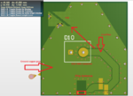
The track I have made is shown in the diagram. Right now the gap between Feed-Ground pour is very narrow.

Thanks in advance
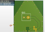
3D_tapered_altium view.png
 

Is there a formula to calculate the distance between Feed and Ground Pour ?
Calculate according to which criterion? The line rather looks like being part of the antenna structure than a clearly defined transmission line.

If both bottom and top copper are acting as pure ground (there should be via fences near the line to assure this), you can calculate the impedance as "coplanar waveguide with ground". But I doubt the assumption is right here. You might want to explain the antenna structure to clarify what is ground and what isn't.
 
Just connsider the via and don't consider the antenna, you can use some sw, such as HFSS, CST,etc., to calculate the via structure.
 

Thanks for your replies. I have labelled the parts in the same picture below
3D_tapered_altium%20view.png
FvM: yes both planes are acting as ground. I thought the VIas i have put are acting as VIA fence for the ground plane. is this not right? Secondly, I have followed the same structure that the manufacturers gave to me for this Chip antenna. This chip antenna is on principle of IFA. Thirdly, how can i make it a clear tranmission line for feed trace? ( I used this formula for feed line width) https://ncalculators.com/electronics/microstrip-impedance-calculator.htm
tony_lth: I thought VIAs have to be simply through the PCB. How would CST help? Determinign the diameter?

Now I found somewhere that for differential pair, if width of trace is 'w' then its distance from GND plane on same layer should be '2w' , what will be true for single trace?

Thanks again
 
Last edited:

Mentioning the chip antenna clarifies what you are doing.

I didn't notice that you had already a via fence along the trace. That's good, but the vias shouldn't have thermal isolation.

Regarding gaps, it's as I already said, the structure has to be calculated as "coplanar waveguide with ground". As a result, the trace width will be considerably reduced for same impedance compared to microstrip line. A good transmission line calculation tool should include coplanar waveguide with ground. Of course , you can do the calculation with a general EM solver as well.
 
Phew this is what I needed, I was using microstrip width calculation tool. I will try removing thermal isolation of VIAs. So far I dont know if Altium allows is, but thats another issue.

Many thanks!
 

If you don't find a suitable calculator supporting "coplanar waveguide with ground" structure, you can post the PCB parameters (thickness, Er, intended impedance and ground isolation)
 

I can use Advanced Design System ADS 2011 . There is a LineCalc tool there. I used this tool **broken link removed**

Which one do you recommend because they give slightly different results. H=1.53 mm ( I subtracted 2 oz copper layer from standard 1.6mm thickness) , T=1 oz ( 0.03479mm), er= 4.61 @ 1MHz. I need to know width @ 1.575 GHz for 50 ohm.
 

Considering the expectable mismatch of a chip antenna and PCB parameter variations, differences of a few impedance percent between tools can be neglected for this problem, I think. I guess that the Polarinstruments tool or an EM solver give correct values, but I never tried to verify it.
 

Status
Not open for further replies.

Part and Inventory Search

Welcome to EDABoard.com

Sponsor

Back
Top