Continue to Site

Welcome to EDAboard.com

Welcome to our site! EDAboard.com is an international Electronics Discussion Forum focused on EDA software, circuits, schematics, books, theory, papers, asic, pld, 8051, DSP, Network, RF, Analog Design, PCB, Service Manuals... and a whole lot more! To participate you need to register. Registration is free. Click here to register now.

[SOLVED] How to Design three level three phase Inverter?

Status
Not open for further replies.

electroM

Member level 4
Joined
Jul 19, 2013
Messages
72
Helped
11
Reputation
22
Reaction score
11
Trophy points
18
Location
Pune, INDIA
Activity points
384
input is 48v 100Ah battery.
required output is for 1kVA transformer.
How to use diode clamped (NPC) inverter.
how to Design line capacitor?
pls help?????:?:
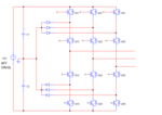
 

input is 48v 100Ah battery.
required output is for 1kVA transformer.
How to use diode clamped (NPC) inverter.
how to Design line capacitor?
pls help?????

How to Design three level three phase Inverter?
Hi
Confusing thread ! title of your thread tells that you want to know how to design a 3level SPWM inverter and then containing literature says that you are looking for something else like how to design or set a capacitor value for that .
If you have a question regarding a circuit , so attach your schematic . if you are looking to know about a topology then ask for it's topology then expect for help .
ok ?
Best Wishes
Goldsmith
 

I want to know how to design a 3level SPWM inverter ???
 

I want to know how to design a 3level SPWM inverter ???
Hi
First of all you need to create two different SPWM signals . first one with message with zero degree of phase shift and 2nd one with the message with 180 degree of phase shift . do you know how to create it ?

Best Luck
Goldsmith
 

I am working with FPGA for generation of SPWM signal. Any tips any suggestions???
 

I am working with FPGA for generation of SPWM signal. Any tips any suggestions???
Hi again
Unfortunately i'm not dealing with FPGA . but i can give you some guide lines .
You can prepare two different signals . first one for positive half cycle and 2nd one for the negative half cycle . ( as you probably know variations of the duty cycle can be cause of variations at the amplitude of the average signal . so both half cycles can be harvested as a pure wave .
Best Wishes
Goldsmith
 
Last edited:

Thanks for reply but problem is with how to drive Gate of IGBT with 5v logic o/p from FPGA?
 

Thanks for reply but problem is with how to drive Gate of IGBT with 5v logic o/p from FPGA?
Hi again
No this is not a problem ! because if you are using a bootstrap driver like IR2113 or 2110 or ... if you use 5 volt as it's vcc and 15 volt as it's vdd it can easily be drove ! it can convert 5 to 15 as well .

Good Luck
Goldsmith
 

can i get some application notes of IR2113 or 2110 for three level three phase inverter or even for how to drive IGBT, what are the parameters to concern for this??
 

can i get some application notes of IR2113 or 2110 for three level three phase inverter or even for how to drive IGBT, what are the parameters to concern for this??
What ?! you can just go to the datasheet4u.com and take their datasheet easily and you'll see how to use them .
By the way for three phase you'll need 3 IGBT driver like that . ( to drive 6 IGBT or Mosfet )
A question did you ever use any IGBT or any mosfet in any kind of power circuit ?

Best luck
Goldsmith
 

Actually previous work is mostly related to the digital logic, micro-controller, FPGA but this is my first work related to the power electronic & Power Devices. therefor looking for a help.
 

how to decide the values of Capacitor C1 & C2 for ckt shown, requires o/p of 24V 42A? Schematic1.png

- - - Updated - - -

how to decide the values of Capacitor C1 & C2 for ckt shown, requires o/p of 24V 42A?
Schematic1.png
 

The question can't be answered without knowing the minimum output frequency.
 
  • Like
Reactions: tpetar

    tpetar

    Points: 2
    Helpful Answer Positive Rating
Actually previous work is mostly related to the digital logic, micro-controller, FPGA but this is my first work related to the power electronic & Power Devices. therefor looking for a help.
Hi again
If you have never drove any kind of mosfet or IGBT i highly recommend you to don't go through this project . first try to design something more simpler with mosfets and IGBTs and this !

Best Luck
Goldsmith
 

Hey Goldsmith I can't. Its my instructor who wants me to do this project. & I'm running short of time.
 

am also try this single phase to three phase inverter but i dont have much knowledge in this circuit design but i try in analog circuit design. could you tell me how to design in analog any circuit for this...
 

how to decide the values of Capacitor C1 & C2 for ckt shown, requires o/p of 24V 42A?

output frequency is 50Hz

Besides minimal output frequency, the energy amount to be delivered from C1 & C2 during clamp diode conduction depends also on the exact modulation scheme. It can be partly compensated by three phase operation of the circuit, but not completely. The best way to determine the exact clamp diode current waveform is a simulation with actual modulation scheme.

There has been a previous discussion about gate control circuits. I presume you already found out that standard bootstrap drivers like IR2110 can't work for a diode clamped multilevel converter.
 

I presume you already found out that standard bootstrap drivers like IR2110 can't work for a diode clamped multilevel converter.


Actually we can use the Two IR2110's as Q11 & Q12 also Q13 & Q14(in single arm) forms two highside & lowside pairs.
 

Status
Not open for further replies.

Part and Inventory Search

Welcome to EDABoard.com

Sponsor

Back
Top