Continue to Site

Welcome to EDAboard.com

Welcome to our site! EDAboard.com is an international Electronics Discussion Forum focused on EDA software, circuits, schematics, books, theory, papers, asic, pld, 8051, DSP, Network, RF, Analog Design, PCB, Service Manuals... and a whole lot more! To participate you need to register. Registration is free. Click here to register now.

Designing a circuit that operates in different paths at different voltages

Status
Not open for further replies.

rahdirs

Advanced Member level 1
Joined
May 22, 2013
Messages
424
Helped
93
Reputation
192
Reaction score
91
Trophy points
1,308
Location
Mordor
Activity points
4,492
Voltage Controlled switch
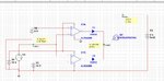
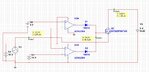
Hi all,

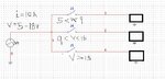
I need to design a circuit that operates in different paths at different voltages.
I have a voltage source whose voltage varies slowly(4 V - 18 V),but it gives out high currents.
I mean i need a kind of voltage dependent switch that does not hinder flow of current.

Eg:If Voltage is at 6 V,the switching circuitry switches to close path 1 & current only flows in path 1
If Voltage is at 9 V,the switching circuit switches on to close path 2,open path 1 & current flows in path 2
.............. for other voltage levels

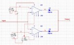
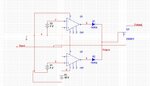
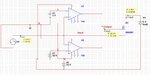
I tried using window comparator with op-amp but op-amps & high currents!!!!!!
 

hi,
use electromagnetic relays with multiple NC & NO contacts . In dc you can choose 5 v relays and zener diodes..... or simply relays with different clamping voltages, to avoid destroying lower voltage relays, use series light bulbs eg. 5 v relay when 18 v supply is present. In this case you need to experiment to get the adequate relay with the adequate light bulb in order to obtain your desired threshold values, the setup its a little bulky, but you get a simple & reliable circuit ...
Of course things can be complicated ... you can use a microcontroler with ADC to measure supply voltage and command some comutation circuits to choose the supply paths, based on the threshold values programmed in it ....this implies more bulky things to do ...
 
Last edited:

You should be able to do that with a window comparator driving logic-level type power P-MOSFETs.
 

How many different voltage levels at what current level do you want to switch?

A simple solution for multiple levels might be an LM3914 dot/bar display where each IC can do ten steps (outputs). Instead of lighting lamps according to the voltage input, you could drive P-MOSFETs from the outputs to switch to the various loads. A large power MOSFET can have an ON resistance in the few tens of milliohm range so its voltage drop when ON can be quite small.
 

How many different voltage levels at what current level do you want to switch?
The current is in range of 10 A & there are 3 levels of voltages.
How do you intend to use MOSFETS for voltage controlled switching
 

Attachments

  • Capture.JPG
    Capture.JPG
    135.8 KB · Views: 90

Which particularly problem do you refer to?

The problem can be divided into three partial tasks:
- decision block, essenstially 9 and 15 V comparator and logic
- level conversion providing suitable gate drive levels
- power switching, e.g. with PMOSFETs

Each of this can be implemented with standard electronic means, some details still need specification, e.g. is reverse conduction of the switches acceptable?
 

The problem can be divided into three partial tasks:
- decision block, essenstially 9 and 15 V comparator and logic
- level conversion providing suitable gate drive levels
- power switching, e.g. with PMOSFETs
@FvM,@crutschow: Ok,i'll use 3 window comparator as in schematic(obviously,other two with different window voltages).Now,how would i allow the 10 A of current to pass from input to output.The op-amp wouldn't let the current to pass from i/p to o/p.
Now how would i use PMOSFETs,can u show a blue-print
 

Attachments

  • Capture.JPG
    Capture.JPG
    95.9 KB · Views: 73
Last edited:

.............................
How do you intend to use MOSFETS for voltage controlled switching
For positive voltages you can use P-MOSFETs with the source connected to the positive voltage and the drain connected to the load. You ground the gate to turn it on and connect the gate to the source terminal voltage (through a resistor) to turn it off. The gate can be controlled by the output of the comparator which is either high (at source voltage) or ground.
 

@crutschow: are you talking about something like the schematic attached.Input is always positive.As i attached source terminal to input when MOSFET is on,does the current of 10 A pass from input to output ??. But i don't think 10 A through a single MOSFET is OK. Maybe i should connect them in parallel to reduce current in each of them.

Also i read on EdaBoard that if you plan to use power mosfets , then prepare for nightmares interms of driver circuit and ESD protection + sparks and a lot of smoke,so is it better to use BJTs??

This,i think is a window-comparator question but how do i take its output to zero when i/p is not in between 5 v & 9 v.Definetely not possible in schematic as V- is GND,but if V- is negative is it possible??
 

Attachments

  • Capture.JPG
    Capture.JPG
    153.2 KB · Views: 77
Last edited:

That would work with some changes:

1. The plus supply voltage goes to the source and the load to the drain of the P-MOSFET, not as you show.

2. You can use a single P-MOSFET if it is a high current device (likely 25A or higher) with a low ON resistance to handle 10A with the low voltage drop you want.

3. The P-MOSFET must be a logic-level type device that will fully turn on (above the Vgs threshold voltage) with a Vgs equal to the lowest supply voltage you will have.

4. The op amp must be a rail-rail type device for use with a single supply. If you use the 741 you will need dual supplies. If the MOSFET gate is pulled negative (rather than ground) to turn it on, that's OK as long as the gate-source voltage doesn't exceed the maximum (typically 20V).

MOSFETs are generally no more susceptible to ESD than a bipolar transistor (except for the gate voltage). I would stay with MOSFETs since they are easier to drive.
 

1. The plus supply voltage goes to the source and the load to the drain of the P-MOSFET, not as you show.
If i connect the plus supply to source,then the current to the load,would come from plus supply.
But,i want to supply current from input,so i think the source should be connected to input or are there any problems in doing so,it would affect voltage appearing at load ??

The voltage at the drain,can i some-how maintain it constant even if i connect source to input which is varying????

The drain would go to the load,i did not complete schematic.
 
Last edited:

If i connect the plus supply to source,then the current to the load,would come from plus supply.But,i want to supply current from input,so i think the source should be connected to input or are there any problems in doing so,it would affect voltage appearing at load ??

The drain would go to the load,i did not complete schematic.
By "plus supply" I meant the input. Sorry for the confusion.

So you understand that the MOSFET in your schematic should have the source and drain reversed. :?:
 

Thanks & i also left V+ pin open,but some-how my window comparator doesn't seem to work.Even for voltages in the range of 5 v - 9 v,current doesn't seem to flow from source to load.The output of window-comparator is also high when it should have been low. There is also a very large voltage drop from source to drain.
 

Attachments

  • Capture.JPG
    Capture.JPG
    146.5 KB · Views: 79

As I stated (you did read my other posts?) you need to either use a rail-rail single-supply op amp or use a dual power supply with a 741.

Also the 2N6851 has an ON resistance of 0.8Ω and is rated for 4A maximum. You need a larger MOSFET with a smaller ON resistance for 10A.
 

@crutschow,@FvM: Yes,now i changed op-amp from 741 to AD 822:Single Supply, Rail-to-Rail Low Power FET-Input Op Amp, & i also changed PMOS to a Single P-Channel Power MOSFET 60V 27.5A 82 mOhm.

But,see the first schematic is simple window comparator without PMOS attached & it works fine i.e. o/p is low,when input is in window,but after i connect the PMOS & LOAD as in schematic 2 the o/p of window comparator doesn't drop even if i/p is within that window.

What am i missing here ?? The i/p are quite far from both supply rails.
 

Attachments

  • Capture.JPG
    Capture.JPG
    154.9 KB · Views: 73
  • Capture1.JPG
    Capture1.JPG
    140 KB · Views: 76
Last edited:

@crutschow: So,this is how the switch operates,when input is within the window of comparator the o/p of window comparator becomes low,turning PMOSFET on & allowing current to pass from Source to Drain.
Is there a way to reduce the voltage drop that occurs between Source & Drain.I am currently getting VDS = -3.00 V.Is there a way to reduce this drop in voltage.
 

Voltage drop depends on Rdson, Vgs threshold and applied Vgs in on-state. There's nothing misterious about it. For really high currents, it might be reasonable to use NMOSFETs and a small (e.g. using charge pump principle) voltage converter that generates a positive gate driver voltage on top of Vin.
 

Status
Not open for further replies.

Part and Inventory Search

Welcome to EDABoard.com

Sponsor

Back
Top