Continue to Site

Welcome to EDAboard.com

Welcome to our site! EDAboard.com is an international Electronics Discussion Forum focused on EDA software, circuits, schematics, books, theory, papers, asic, pld, 8051, DSP, Network, RF, Analog Design, PCB, Service Manuals... and a whole lot more! To participate you need to register. Registration is free. Click here to register now.

Error while flooding in PADS

Status
Not open for further replies.

vivek20055

Banned
Joined
Nov 4, 2012
Messages
39
Helped
1
Reputation
2
Reaction score
1
Trophy points
1,288
Activity points
0
Hi,


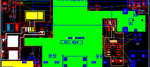
I am getting a error while flooding in PADS.

I am attaching the file of error with this message

Can anyone help me in understanding this error???

And how can I flood all the plane areas at a time in PADS???


Regards,
Vivek Alaparthi

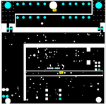
THERMAL RELIEF ERRORS REPORT -- Ind_Hea 3.pcb -- Tue Jan 29 09:21:04 2013


Drilled pads with Nondrilled pads with
less than 50% thermal extensions less than 50% thermal extensions

Report of Thermal Spokes Generator.

On GND Layer:
(60.35, 28.45) # = 0
(20.27, 32.26) # = 0
(19.4, 28.76) # = 0
(28.04, 30.69) # = 0
(26.95, 26.41) # = 0
(24.93, 24.82) # = 0
(23.51, 25.9) # = 0
(56.41, 29.04) # = 0

Total Drilled pads: 8 Total Nondrilled pads: 0
 
Last edited by a moderator:

Hi vivek ,

it is not error this is thermal spoke generation usually spoke must four wheel only in your it is assign less then four.

for floor plane you have to follow this step
1.first select the layer type split/Mixed in setup--> Layer definition,then Assign Net tab is enable select the net (which net you need to assign the shape like VCC,Gnd )
2.draw the shape using Plane area icon and then it will ask the net name choose it
3.tools-->pour mananger-->plane connect select the layer apply copper
try this it will help u..
 
Hi

Thank you for your reply kapil

I tried it and it is working

But only some are flooded and some are not flooding.why?

Regards,
Vivek Alaparthi
 

Hi vivek
select shape and then right click select net you will come to know whether net has assigned or not for particular net
 

Hi kapil,

I checked, but everything is fine. I have assigned nets to every plane area and I used pour manager for connecting planes.

I am attaching a image with this message

- - - Updated - - -

Hi kapil,

I checked, but everything is fine. I have assigned nets to every plane area and I used pour manager for connecting planes.

But some plane areas are connecting with copper while some are not. I do not undersstand. why???

I am attaching a image with this message

- - - Updated - - -

Hi kapil,

I checked, but everything is fine. I have assigned nets to every plane area and I used pour manager for connecting planes.

But some plane areas are connecting with copper while some are not. I do not understand

I am attaching a image with this message

- - - Updated - - -

Hi kapil,

I checked, but everything is fine. I have assigned nets to every plane area and I used pour manager for connecting planes.

But some plane areas are connecting with copper while some are not. I do not understand

I am attaching a image with this message
 

Attachments

  • PLANE AREAS.png
    PLANE AREAS.png
    36.1 KB · Views: 123
  • PLANE AREAS.png
    PLANE AREAS.png
    36.1 KB · Views: 124

Hi kapil,

Thanks for your reply and patience

I tried it and it worked perfectly

Can you please tell me the difference between plane areas, copper and copper pour.

I have different supplies like 24v, 3.3v,5v and 12v in my schematic.

So, which method is good in my case. Is it plane area or copper pour or copper area


Regards
Vivek Alaparthi
 

Hi vivek
in my point of view better use plane area only because if you use plane area while pouring everything is pouring at that time.
 
  • Like
Reactions: vivek20055

    V

    Points: 2
    Helpful Answer Positive Rating

    vivek20055

    Points: 2
    Helpful Answer Positive Rating
I need to increase copper thickness in all the layers. So, in layer setup---->thickness dialog box. I have component,substrate(prepeg),coating for all the layers. which parameters I need to change to increase the thickness of copper. I am attaching a image with this mail.


Regards,
Vivek Alaparthi
 

Attachments

  • copper thickness.png
    copper thickness.png
    50.8 KB · Views: 170

Hi Kapil,

My professor suggested me to place input supply (which are also high reverse current path devices) at the edge of the board

And use copper flooding in 3 layers (including top,power and bottom)???

For ground layer he suggested to give seperate GND to these components for good return current????

what does that mean ???

what is the idea behind using copper in 4 layers??

Regards,
Vivek Alaparthi
 

Hi vivek,
power supply section should be placed in edge of the board because to reduce noise as well as heat.in your power section may be high current ,need more copper for that power
to reduce noise like EMI and EMC as well as cross talk four layer is good
 

Hi kapil,

what is cross talk 4 layer. Can I use vias for the 4 layers of copper.

But then ground layer will be there in the same path. Right??

Regards
Vivek
 

Hi vivek,
cross talk means two signals are overlapping to each other.you can use via
 

Hi Kapil,

My professor suggested 5mm wide trace in several layers for the input(24V)

But my input contains 24V and 1.5 amperes current(not high current)

So, what is the need of using 4 layers for the input(we can give in just one layer. Right?)

But this input goes to inductor and then tank capacitors(LC circuit).

Both ends of capacitors are connected mosfets. These Mosfets switching on/off alternatively with the help of controller.

So due to magnetic flux high current will be produced into the coil for welding purpose.

But, I dont understand,what is the need of using 4 layers for the input(we can give in just one layer. Right?)

Regards,
Vivek Alaparthi
 

Attachments

  • cicuit1.png
    cicuit1.png
    155 KB · Views: 93
  • pcb1.png
    pcb1.png
    40.5 KB · Views: 92
Last edited:

Hi vivek,

For your input i understand why your professor prefer 4 layer ,the following things you need to consider,

1.no of components and no of nets need to consider.(see in your design has USB,QFN ,MOSFET ) for routing.in USB it is need at least 2 layer like that each component need to consider
2.depends on board size layer count may be vary .(if board size is big we can try it in 2 layer).
3.mostly no of nets (power,critical nets,clock net) as well as board size impact the layer count .in case in your design has more amount of power nets is there so that only they prefer 4layer
4.depends on application. this also important role for choosing 4 layer

Hi,

For the GND layer I have given seperate (GND) ground for high current path(from transistors) which is connected to normal GND at a point.

I have given the seperate analog ground(AGND).

My professor commented like this:

What is this separation for the ground used for?

Looks strange to me. The upper part will be more fluctuating.

If you only have analog parts over the analog GND then it is good that you are using a separate analog gnd but I am surprised that the analog part is so spread. A problem might be that your analog GND is connected at the end of the digital GND and digital noise will be added to your analog gnd. A start connection to the common GND separation might improve.


what does this mean?????

How can I add start connection???

I am adding image with this message

Regards
Vivek Alaparthi
 

Attachments

  • GND.png
    GND.png
    35.1 KB · Views: 101
Last edited:

Status
Not open for further replies.

Part and Inventory Search

Welcome to EDABoard.com

Sponsor

Back
Top