zakkos
Newbie level 6
Hello everybody,
a friend of mine is repairing a samsung galaxy note 2 and has some trouble identifying a broken component.
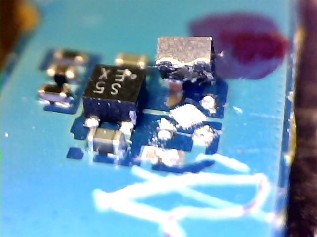
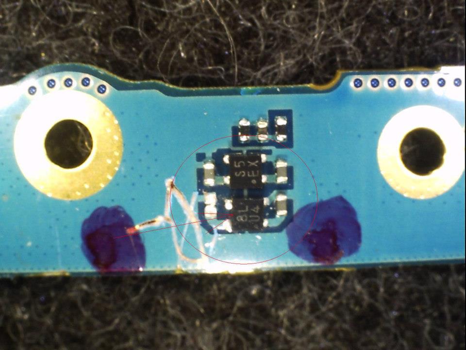
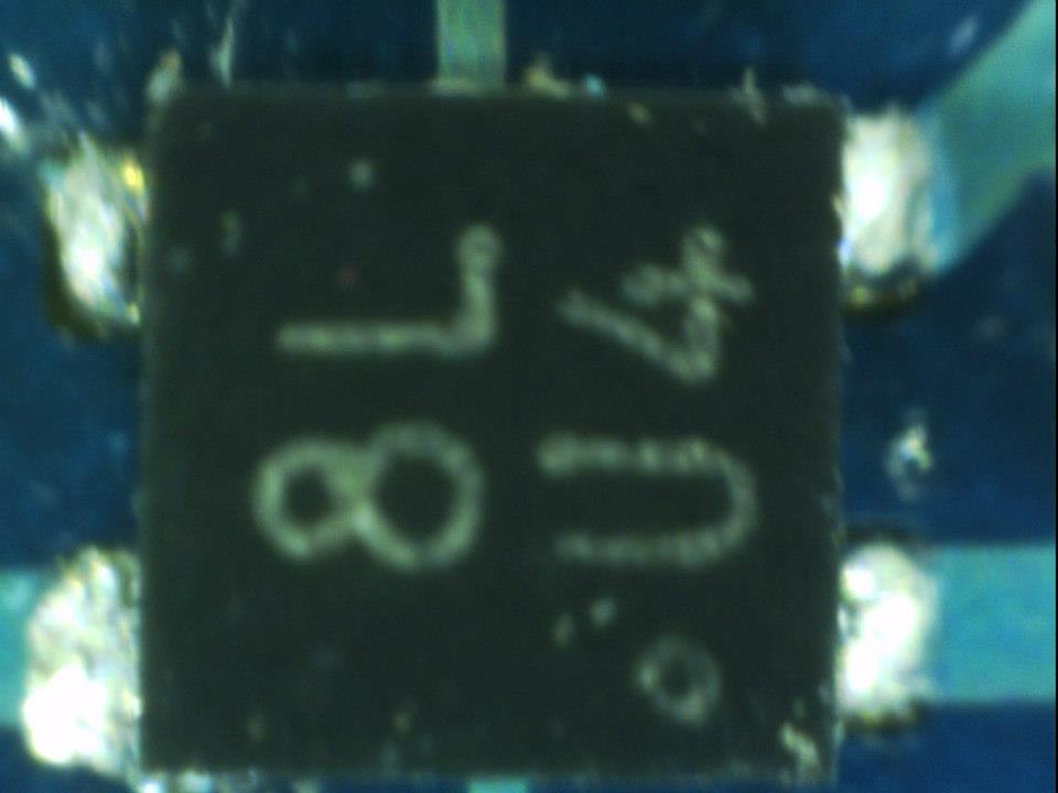
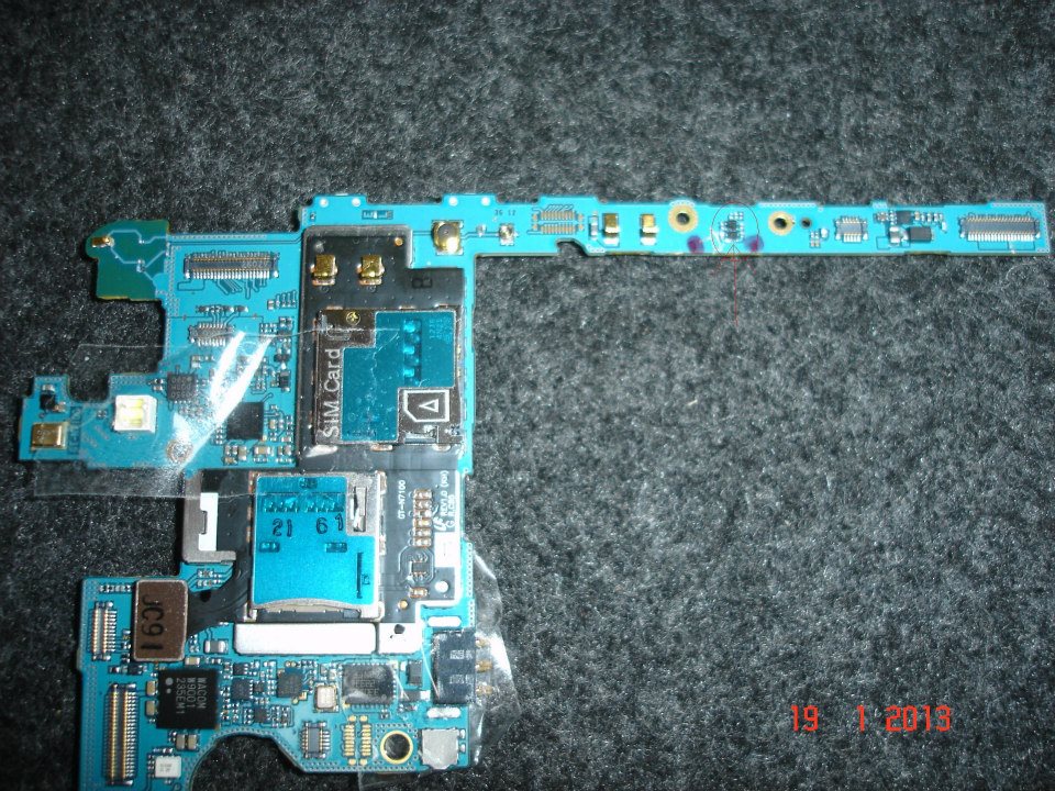
It has 4 pins plus a central one which i suppose is ground plus anchorage, smd with an almost cubic package. It's marked 8LU4 in a 2x2 fashion (8L on top and U4 below) and a simple search on google and various IC finding sites didn't end up with something useful. Right next to the broken component looks like there is another one of the same kind marked S5EX (as you can see in the picture). Can someone help me identifying those components? Alternatively are schematics of this phone available (again a google search returned no results...) to track the component down?
Thank you in advance!
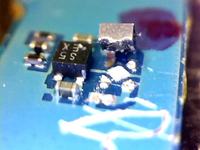
a friend of mine is repairing a samsung galaxy note 2 and has some trouble identifying a broken component.
It has 4 pins plus a central one which i suppose is ground plus anchorage, smd with an almost cubic package. It's marked 8LU4 in a 2x2 fashion (8L on top and U4 below) and a simple search on google and various IC finding sites didn't end up with something useful. Right next to the broken component looks like there is another one of the same kind marked S5EX (as you can see in the picture). Can someone help me identifying those components? Alternatively are schematics of this phone available (again a google search returned no results...) to track the component down?
Thank you in advance!