calp
Newbie level 2
hi all,
I ve been searching thru the similar threads, and I see that there is not a clear consensus on the way we can define the ports in momentum simulation setup for ads version 2011; (NOT the 2009 version).
My question -however it may sound silly- is as follows with the figure below:
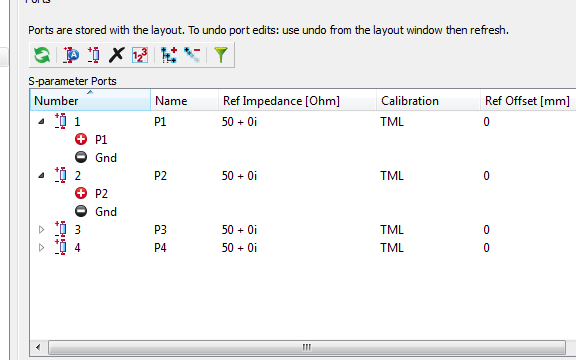
In this figure the orange colored line is a thick top metal, 200 um long, 16 um wide... the blue outline is actually a metal 1 layer underneath the top metal... This Metal 1 will be connected to the ground using substrate contacts later in the system level. It is a simple microstrip line with Metal 1 ground... (my pin placement may be wrong, so pls feel free to comment on them as well)
Well, the substrate has a cover layer way below the metal 1 and it seems like the ads 2011 assigns the universal ground to that layer... (GND)
So, how can i override this GND assignment? How do I confine my analysis of this transmission line to these Topmetal and Metal 1 layers?
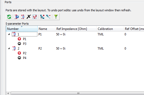
From my preliminary simulations, I ve noticed that the TML or None options inthe port setup have significant effects on the characteristics of this TLine (S11 has 20 dB difference in level for the two cases, and it seems that my TLine can oscillate on its own at 70 GHz! just by itself when I select TML calibration mode with all ports are referenced to GND individually... pls see the figure: the blue line is the TML options checked. The pink line is when you group two metal 1 ports and assign them to the negative terminals of port 1 and port 2 of the topmetal.)
I hope I ve made myself clear enough. If not, you can try out a similar structure and test it with various combinations and notice the differences...
So the question is where do I go wrong? and how do we set the alternate ground plane without modifying the substrate that comes with the PDKs.
thanks in advance
I ve been searching thru the similar threads, and I see that there is not a clear consensus on the way we can define the ports in momentum simulation setup for ads version 2011; (NOT the 2009 version).
My question -however it may sound silly- is as follows with the figure below:
In this figure the orange colored line is a thick top metal, 200 um long, 16 um wide... the blue outline is actually a metal 1 layer underneath the top metal... This Metal 1 will be connected to the ground using substrate contacts later in the system level. It is a simple microstrip line with Metal 1 ground... (my pin placement may be wrong, so pls feel free to comment on them as well)
Well, the substrate has a cover layer way below the metal 1 and it seems like the ads 2011 assigns the universal ground to that layer... (GND)
So, how can i override this GND assignment? How do I confine my analysis of this transmission line to these Topmetal and Metal 1 layers?
From my preliminary simulations, I ve noticed that the TML or None options inthe port setup have significant effects on the characteristics of this TLine (S11 has 20 dB difference in level for the two cases, and it seems that my TLine can oscillate on its own at 70 GHz! just by itself when I select TML calibration mode with all ports are referenced to GND individually... pls see the figure: the blue line is the TML options checked. The pink line is when you group two metal 1 ports and assign them to the negative terminals of port 1 and port 2 of the topmetal.)
I hope I ve made myself clear enough. If not, you can try out a similar structure and test it with various combinations and notice the differences...
So the question is where do I go wrong? and how do we set the alternate ground plane without modifying the substrate that comes with the PDKs.
thanks in advance