Continue to Site
Follow along with the video below to see how to install our site as a web app on your home screen.
Note: This feature may not be available in some browsers.
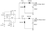
It works only for the positive rail.
When the 555's output is low it's at 0V (the Earth in your diagram). The output labelled "negative voltage output" produces nothing.
If an opamp is needed to be powered by this circuit, the two rails must have equal opposite voltages. Since this circuit's voltage will degrade as current increases, one can never maintain a similar voltage to the negative one, if taking that voltage directly from the vcc. an identical positive rail to the negative one must be used, to maintain voltage balance. I can see it this way.Hmmm, now I'm a bit confused myself, but about the positive output works. Additionally, I don't see the necessity for it. Why not use the positive rail to the 555 directly?

I think D1 anode should be connected to +ve to get a more +ve voltageHmmm, now I'm a bit confused myself, but about the positive output works. Additionally, I don't see the necessity for it. Why not use the positive rail to the 555 directly?
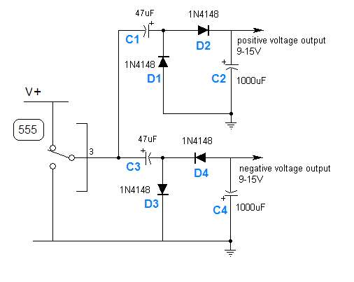
Let's see what's happening. I've shown the output of the 555 as a switch which connects pin 3 to either the supply rail or to 0V.
I don't understand the purpose of C1 and D1.