jegues
Member level 3
Hello all,
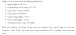
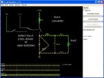
See figure attached for requirements regarding a design problem I am working on, in addition to my work thus far.
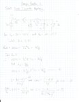
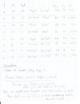
I've managed to come up with a number of equations for my component values but they all contain parameters that have varying ranges.
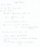
Is it possible to write enough equations to correctly solve for everything simultaneously or do I need to select a particular parameter as a starting point are work outwards from there?
I need to preform a worst case design so it must meet the design criteria in the worst case scenarios. How can I identify what these worst case scenarios are?
Thanks again!
See figure attached for requirements regarding a design problem I am working on, in addition to my work thus far.
I've managed to come up with a number of equations for my component values but they all contain parameters that have varying ranges.
Is it possible to write enough equations to correctly solve for everything simultaneously or do I need to select a particular parameter as a starting point are work outwards from there?
I need to preform a worst case design so it must meet the design criteria in the worst case scenarios. How can I identify what these worst case scenarios are?
Thanks again!