Continue to Site

Welcome to EDAboard.com

Welcome to our site! EDAboard.com is an international Electronics Discussion Forum focused on EDA software, circuits, schematics, books, theory, papers, asic, pld, 8051, DSP, Network, RF, Analog Design, PCB, Service Manuals... and a whole lot more! To participate you need to register. Registration is free. Click here to register now.

Gm-c bandpass filter transient response

Status
Not open for further replies.

lhlbluesky

Banned
Joined
Mar 30, 2007
Messages
558
Helped
5
Reputation
10
Reaction score
5
Trophy points
1,298
Location
china
Activity points
0
i have designed a Gm-C BPF, biquad type with two OTA and two Cap. i set gm1=gm2=gm=13uS (low power design), C2=100*C1=1nF, f0=gm/sqrt(C1*C2)=20kHz, Q=sqrt(C2/C1)=10, now, the ac response shows that, f0 and Q has some deviation (20.4KHz and 9.23), what is the possible reason here?

besides, for a Gm-C BPF, how is the transient response? does the OTA need slew rate and settling (the same as OPA)? if so, for a 1nF cap, it is very difficult for the OTA to settle well. am i right?

thanks all.
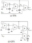
 

i have uploaded the BPF fig, TFS and GFS. but i have some questions in transient simulation.
1, for TFS, the AC response shows that, f0=20.4KHz(ideal 20KHz), Q=9.23(ideal 10), H0=0.5(ideal 1). when transient simulation(an AC coupling cap added before VIN), the virtual ground is 0.8V(positive input of g1 and negative input of g2), and i add a 20KHz sine wave(0 to 0.2V pk-pk), but vout is only 0.5V or so (and very slowly increasing). why? any mistakes here? C1=10pF, C2=1nF, gm1=gm2=gm3=13uS.
2, for GFS, the AC response shows that, f0=20.5KHz(ideal 20KHz), Q=9.28(ideal 10), H0=0.4(ideal 1). when transient simulation(an AC coupling cap added before VIN), the virtual ground is 0.8V also, and i add a 20KHz sine wave(0 to 0.2V pk-pk), but vout is only 0.2mV pk-pk sine wave(dc offset=0.78V, not 0.8V). and why H0 becomes so small (1/1000)? any mistakes here? C1=10pF, C2=1nF, gm1=gm2=gm3=13uS.
thanks.
3.jpg
 

Ihlbluesky, some comments/questions:
* You cannot expect virtual ground at OTA inputs (applies only to voltage opamps).
* are values for transconductances gm measured or calculated?
* deviations caused by imperfections (finite Rout of OTA`s)
* Capacitor spread very large! (10 pF to low at the OTA output, influence of parasitic capacitances).
 

values for transconductances gm is measured. and is there any other mistake in my design?
 

in my ac simulation, H0=0.95(ideal = 1), but in transient simulation, it is only 0.1 (a little increase with decreasing of input pk-pk), what is the non-ideal factor of influencing H0 in transient simulation? slew rate and bandwidth? in my view, f0=gm/C, and gm and C are proportional, if i increase gm, C will increase the same amount, to make constant f0. so, how to consider settling of OTA (and the whole BPF)?
besides, if i use switched-cap structure for BPF design, what is the proper choice, MFB, sallen-key, or others? and how to simulate the ac characteristic of switched-cap BPF (with two clock phase at least)? such as AC response, noise, thd, etc.
for the f0 control, we can change the clock frequency of swithes, the clock can be generated by an frequency-tuning oscillator, and any other methods to generate switched clock?
thanks.
 

Ihlbluesky, I only can guess what you mean using the abbreviation "Ho". Why don`t you use words to avoid misunderstandings?
Repeatadly, I have mentioned the finite output resistance of the OTA. Why don`t you comment on this with some details?
I also have mentioned already the very large capacitance spread of 1000/10=100, which should be avoided.

In my view, f0=gm/C, and gm and C are proportional, if i increase gm, C will increase the same amount,

C will increase? Automatically? I don`t understand.

In case of S/C filter structures you cannot use Sallen-Key or MFB topology. There are specific structures, which are especially suited for S/C applications (based on integrators).
 

thanks. H0 is the passband max gain when f=f0. about OTA, if i want to tune f0 (center frequency) linearly by a resistor, what structure should i use? and for constant f0, gm and C must be change in the same ratio, that is what i mean.
about S/C bandpass filter, based on integrators, can you give me some advice (for two-order)? and should i use z-domain analysis for S/C filter design?
thanks.
 

about S/C bandpass filter, based on integrators, can you give me some advice (for two-order)? and should i use z-domain analysis for S/C filter design?
thanks.

I am afraid, a forum like this is not the right place for a lesson on S/C techniques. There are dozens of papers and introductory articles, which can be downloaded from the internet.
In general: For a detailed mathematical treatment of S/C filters you need the z-transformation - however, not for designing a second order filter because one can rely on existing formulas and design rules.
 

i now found that, in ac simulation, there is a LHP zero at low frequency, i think it is generated by the finite output resistance of OTA, right? and can this zero have an influence on the transient response of the BPF above mentioned?
 

Sounds unlikely for a regular OTA topology.

Yes, I agree - and I am curious how this zero was identified?

- - - Updated - - -

More than that, I would like to know
* are your results based on simulation only?
* if hardware related - lumped elements or IC technology?
* real (finite) OTA input and output impedances?
 

yes, it is based on simulation only. and it is identified in ac amplitude and phase response, the LHP zero is at 20Hz or so, is there something wrong?
 

yes, it is based on simulation only. and it is identified in ac amplitude and phase response, the LHP zero is at 20Hz or so, is there something wrong?

Ihlbluesky, in post#4 you have told us that the transconductance was "measured". Now we hear that the results are based on "simulation only".
I hope you see that it is not easy to help you without sufficient information.
Why don`t you proceed systematically?

You have two structures to work with.
*At first - you should simulate the circuits with IDEAL OTA`s (VCCS) in order to convince yourself that the selected topologies work as (theoretically) predicted.
Thus, it is not necessary to ask us if there is any error in your design (as you did in post#4).
*As a second step, you use real OTA models (finite input/output impedances) in order to identify the deviations from the ideal case.

If the results do not satisfy you and if you ask for some help you must inform us about the circuit details - in particular, the OTA model and its properties.
Don`t you think that such an approach could lead to meaningful results?
 
  • Like
Reactions: FvM

    FvM

    Points: 2
    Helpful Answer Positive Rating
sorry, the results are based on simulation only, it is my fault for the mislead of you.
the circuit is as post#2 shows, the four-OTA topology. and the OTA is just simple five-transistor structure with input pair working in weak-inversion region.
thanks.
 

Status
Not open for further replies.

Part and Inventory Search

Welcome to EDABoard.com

Sponsor

Back
Top