Continue to Site

Welcome to EDAboard.com

Welcome to our site! EDAboard.com is an international Electronics Discussion Forum focused on EDA software, circuits, schematics, books, theory, papers, asic, pld, 8051, DSP, Network, RF, Analog Design, PCB, Service Manuals... and a whole lot more! To participate you need to register. Registration is free. Click here to register now.

Regarding RF attenuator linearity

Status
Not open for further replies.

cjrathi

Member level 2
Joined
Oct 18, 2012
Messages
52
Helped
0
Reputation
0
Reaction score
0
Trophy points
1,286
Activity points
1,704
Hi,
I am trying to improve the linearity of 90 dB digital attenuator. Its performance is non-linear at high attenuation level. What improvement or rather which circuitry can be added in the schematic to improve it. Please suggest some relevant document.


Thanks
Chaitanya
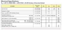
 

"Performance is non-linear at high attenuation levels". Without a circuit, IC device number or frequency its hard to help you. How does what you are seeing compare with the manufacturers data sheets? Are you sure that you are not bypassing signals around the attenuator? 90 dB is a lot, should require very good screening and layout.
Frank
 

Thanks Frank ..

Actually 90 dB attenuator is designed by cascading 3 digital attenuator ICs (Hittite HMC425LP3), whose attenuation level is controlled by Control signals from software..

The problem with this design is that , as I said, it is non-linear after when i give attenuation of 60 dB. Is there any circuitry that i can add which will avoid this ? Atmost care has been taken regarding bypassing, decoupling of signals as per datasheet of IC.


Thanks
Chaitanya

What's your RF Power in ? What are you using to measure the signal ?
If you use signal at 0dBm and try to measure -90dBm on a Spectrum Analyzer you will
loose accuracy, thus making it "Look" non-linear.

Try to increase the input power and see if it "Becomes" linear.
Check the data sheet, you may be operating out side of the intended range of your device.
 

You mean linearity or flatness? If you mean flatness, the result you get is as expected. When you increase the attenuation, gain(negative) flatness worsens as you see from the datasheet and it is not avoidable.
 

Hi,
I am trying to improve the linearity of 90 dB digital attenuator. Its performance is non-linear at high attenuation level. What improvement or rather which circuitry can be added in the schematic to improve it. Please suggest some relevant document.


Thanks
Chaitanya

At this level of attenuation, the layout of CONTROL lines is VERY important.

This cannot be over-emphasized ... it seems to the be the number one mistake designers make, and then it affects amplifier flatness, stability, and even input S11 (input match) when the output feeds back to input on active modules!

So, please pay proper attention to 'decoupling' (using low pass fitler techniques) on your digital (or analog) control lines.

One 'way' to check for adequate isolation of control lines might be to tie all lines to maximum attenuation directly *at* the attenuators and measure the attenuation value ... remember to cut the foil at the attenuator to prevent signal coupling between stages.


RF_Jim
 

I make a 90db digital attenuator with three hmc424lp3. attenuation signals are converted to ttl level with 74hct14. and the attenuators are made in three different boxes.
90db is a lot attenuation and you should have isolation over than 100db to have linear operation.
 

THanks everyone..

DO i need to separate digital control lines and RF path's ground plane to improve the linearity??

Also can i simulate this whole model on ADS?? How do I make this Hittite Attenuator part on ADS?? Is is possible??

@ FRank:- The thing is i cannot change input power.. Input power can be anything near 0 dBm and i need to attenuate it to minimum of -90 dBm..

What should be the possible solution for this non-linearity and fluctuations of attenuation response at high attenuation level...?

Please help..
 

Thanks Frank ..

Actually 90 dB attenuator is designed by cascading 3 digital attenuator ICs (Hittite HMC425LP3), whose attenuation level is controlled by Control signals from software..

The problem with this design is that , as I said, it is non-linear after when i give attenuation of 60 dB. Is there any circuitry that i can add which will avoid this ? Atmost care has been taken regarding bypassing, decoupling of signals as per datasheet of IC.

Thanks
Chaitanya
The linearity of IC attenuator circuits have been defined by manufacturer so that any additional precaution can not be applicable.The nonlinearity comes from its nature and fixed by supply/bias etc.
You may consult to manufacturer..
 

The linearity of IC attenuator circuits have been defined by manufacturer so that any additional precaution can not be applicable.The nonlinearity comes from its nature and fixed by supply/bias etc.
You may consult to manufacturer..

There must be something i would do at least to reduce fluctuations of Attenuation response at high attenuation level..?
 

There must be something i would do at least to reduce fluctuations of Attenuation response at high attenuation level..?


As you see, IIP3 is defined well under some circumtansces.
But I just want to get your attenuation algorithm.How have you used it ?? Because you shouldn't exceed the mentioned power levels at each input of three attenuator, so input powers should be organized so that nonlinearity of each attenuator shall be in-spec.

Definitely input power to those attenuator parts is well within IIP3 level. While testing it on VNA i set the RF input power to 20dBm which is within its range..

Do this anything have to do with mixed signals on same PCB board., i.e, RF and digital signals.. ? Is there anything i could do to separate them ?
 

Attenuation Error has relation with attenuation of each chip. but at high attenuation levels(~70dB) the isolation is dominant and you must isolate the Power supply and control signals of different attenuators. and also you should take care to pcb layout for having good isolation between the first attenuator input to the last attenuator output.
 

Okay i will try that.... Does the RF trace width should be set as per the frequency of the RF or we can set anything as per the space requirement on board?
 

Definitely input power to those attenuator parts is well within IIP3 level. While testing it on VNA i set the RF input power to 20dBm which is within its range..

Do this anything have to do with mixed signals on same PCB board., i.e, RF and digital signals.. ? Is there anything i could do to separate them ?
Digital signals should absolutely be seperated to minimize the influence of noise but digital signals don't impact-either improvement or degredation-the nonlinearity.Instead, you should organize the controller algorithm so that max. RF power wouldn't exceed specified values.Let me give you an example..
Let say you need 70dB attenuation.You may choose those configurations..

0+35+35 or 20+25+25 or any combination of these values.Think about that..
With a proper algorithm, you will able to maintain the max. admissible RF Power at each attenuator block that has been defined in the table in terms of linearity.
 

In my design what i have done is that out of 8 digital control lines coming from computer, 6 lines are connected to first ATT part( So it will give attenuation of full range from 0 to 31 dB) and other 2 are given to next two parts each ( SO they will give either no or full attenuation ). For sure, RF input power at each ATT parts is within its acceptable range...
 

Its performance is non-linear at high attenuation level.

Maybe the others have the same confusion that I have: What linearity to do mean?

Linearity vs. input power
or linearity of attentuation vs. the nominal value
or flatness of attentuation vs. frequency
 

I guess, Chaitanya is referring to "linearity of attentuation vs. the nominal value", the quantity that is designated "attenuation accuracy" in the above quoted datasheet. I would prefer this much clearer term.

PS: As an additional point, I'm completely missing any quantitative attenuation results, frequency range, information about circuit layout. It's almost useless to discuss the problem at this level of information.
 
Last edited:

Untitled.png


Here are my readings... As u can see at % GHz band after 70 dB of ATTN level, actual attn varies a lot. This needs to be stabilized.. Please suggest some solution to this..
 

At first sight, the results suggest incorrect level measurement.
 

Status
Not open for further replies.

Part and Inventory Search

Welcome to EDABoard.com

Sponsor

Back
Top