adnan012
Advanced Member level 1
hi,
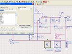
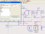
i am confused in finding the optimum load impedance for SD57060.
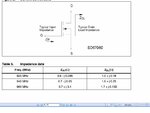
As shown on SD57060 LOAD IMPEDANCE.JPG (taken from SD57060 DATASHEET)
at 945MHz the ZL is 1.6+j*0.25
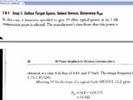
on book.JPG
there is a formula to determine load impedance.
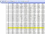
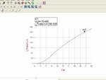
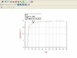
on sparameters.JPG (taken from SD57060 DATASHEET)
VDD = 28V
IDS = 2A
S22 = 0.978 -168.77
This gives zout=50*((1+polar(0.978,-168))/(1-polar(0.978,-168))) //equation in ADS
Zout = 14ohm
if the formula is correct.
why this information is given with VDD and ids? does it follows the Ropt=(Vdgb-|Vp|-Vk)/IDSS formula for class AB AMPLIFIER along with class A amplifier.
What is the actual optimum load for SD57060?
What is Zl as show on SD57060 LOAD IMPEDANCE.JPG?
Why ADS LSSP shows s22 1.6+j*0.25 at 945MHz?
Which value should be used for LOAD PULL TEST?
i am confused in finding the optimum load impedance for SD57060.
As shown on SD57060 LOAD IMPEDANCE.JPG (taken from SD57060 DATASHEET)
at 945MHz the ZL is 1.6+j*0.25
on book.JPG
there is a formula to determine load impedance.
on sparameters.JPG (taken from SD57060 DATASHEET)
VDD = 28V
IDS = 2A
S22 = 0.978 -168.77
This gives zout=50*((1+polar(0.978,-168))/(1-polar(0.978,-168))) //equation in ADS
Zout = 14ohm
if the formula is correct.
why this information is given with VDD and ids? does it follows the Ropt=(Vdgb-|Vp|-Vk)/IDSS formula for class AB AMPLIFIER along with class A amplifier.
What is the actual optimum load for SD57060?
What is Zl as show on SD57060 LOAD IMPEDANCE.JPG?
Why ADS LSSP shows s22 1.6+j*0.25 at 945MHz?
Which value should be used for LOAD PULL TEST?