jasonc2
Full Member level 4
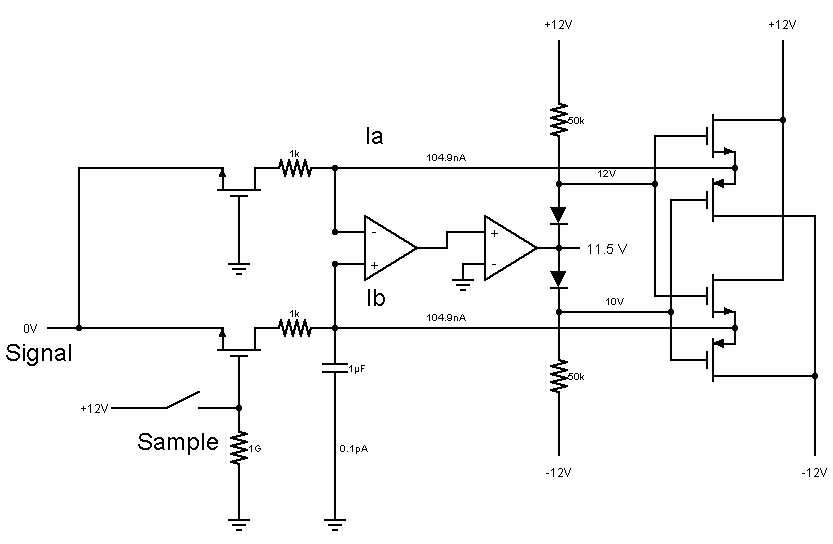
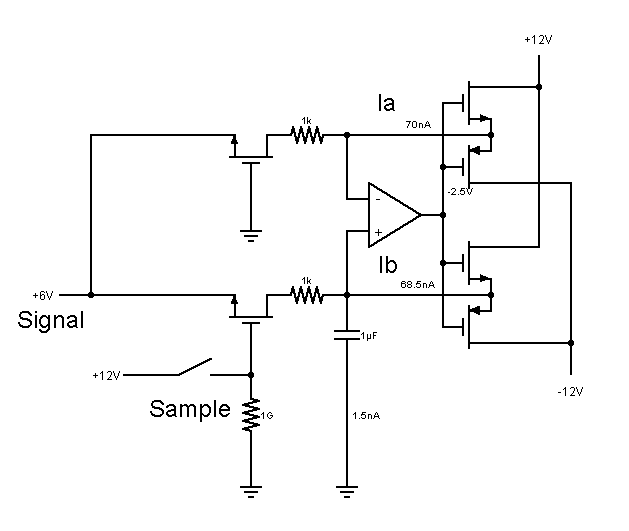
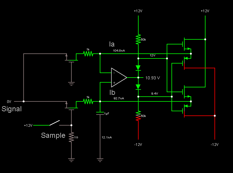
I am playing with sample+hold circuits in pspice and after getting frustrated with leakage currents across mosfet hold switch I went to falstad and tried to come up with a way to compensate for the leakage using ideal and identical components. Here is part of an sh circuit (hold switch + capacitor + attempt at correction):
Falstad simulator link: https://tinyurl.com/cstu8w6
On the left, the bottom mosfet is the switch and the top is identical with 0 gate voltage. The op amp tries to eliminate current through capacitor by adjusting the mosfets on the right to allow a compensating current to pass. "Ia" is the current flowing through the 0 gate mosfet, "Ib" is the compensation current and ideally it equals Ia when the hold switch is off.
To play with it adjust the "signal" slider on the right and hold down the "sample" switch (which I should have labelled "hold") for a little while to take a sample. Bottom left scope shows capacitor voltage and current, center is Ia, right is Ib.
It reduces the leakage (note I'm also assuming an ideal capacitor and only compensating for mosfet leakage) by a factor of 10 to 100 depending on the signal and hold voltages, but as you can see Ia is not equal to Ib and so there is still leakage (the magnitude of Ia-Ib also differs depending on the state).
Why is this happening? Am I missing some fundamental thing here? I don't quite understand what is going on that is causing the currents to be different despite all of the mosfet and resistor models being identical.
Thanks!
") .
.