nodee
Junior Member level 3
Hi,
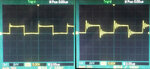
We have recently moved our design onto a PCB but have encountered problems with what looks to be noise on a switching signals from one IC, the IC is a 125kHz antenna driver for a RFID application. On a prototype board the 125kHz square wave is clean (see picture left) but when on the PCB the signal has a decaying oscillation after each switch point (see picture right).
The PCB is 4 layer with a ground plane in the layer below the switching signals. decoupling caps are probably not as close as they should be on the board but I have also soldered caps directly onto the pins producing no change in the signal noise.
Could anyone suggest what might be causing this and possibly offer a solution?
Thanks,
Nodee