Continue to Site

Welcome to EDAboard.com

Welcome to our site! EDAboard.com is an international Electronics Discussion Forum focused on EDA software, circuits, schematics, books, theory, papers, asic, pld, 8051, DSP, Network, RF, Analog Design, PCB, Service Manuals... and a whole lot more! To participate you need to register. Registration is free. Click here to register now.

DC-offset cancellation in opamp due to mismatches

Status
Not open for further replies.

engrMunna

Advanced Member level 4
Joined
Oct 25, 2010
Messages
106
Helped
6
Reputation
12
Reaction score
5
Trophy points
1,298
Activity points
2,071
Hi,
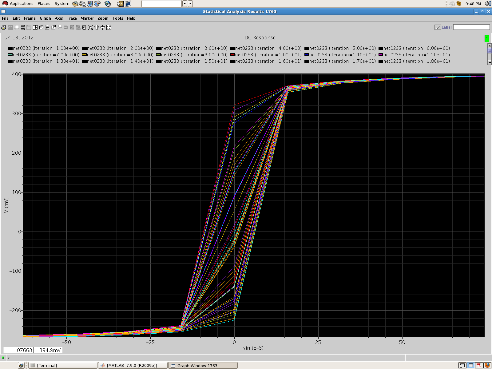
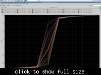
In an op-amp, or a compaarator for that matter, if you plot the input differential voltage vs the output voltage, we get a transfer curve like an inverter. Now if I do montecarlo simulations on transistor mismatches, the output curve is shifted. I am attaching a picture which shows the montecarlo simulation for an opamp where a sweep of the differential input voltage is performed. This offset can cause the op-voltage to stick to one of the rails. Although this off set can be finished by offset cancelation loop, but these loops too require an opamp. My question is that I have never seen commercialy available op-amps with such offset compensation, then how do they work? I mean there is bound to be some mismatch which causes these offsets? Any pointers on how to work round this problem? I have a offset compensation loop but that too would require an opamp?


This offset can cause the op-voltage to stick to one of the rails.
No it doesn't

My question is that I have never seen commercialy available op-amps with such offset compensation, then how do they work? I mean there is bound to be some mismatch which causes these offsets?
Every commercially available op-amp has DC offset. It is specified in the datasheet. See the example below.


Input offset voltage is technique issues. Is impossible manufacture two identical transistor or inpust stage resistor or current source in amplifier.
Exist special amplifier edition with low offset for example https://www.analog.com/static/imported-files/data_sheets/ADA4528-1.pdf with offset 300nV.
in other case is possible use external offset compensation.
 

Certainly if you operate the op amp open loop, then the input offset will cause the output to go to one of the rails since it is multiplied by the large open-loop op amp gain. But in normal closed loop operation the offset simply appears at the output multiplied by the closed loop gain for a non-inverting circuit and (1+ closed-loop gain) for an inverting circuit.
 

Of course, chrutschow is right - and his arguments hold also for the case that there is only capacitive feedback (integrator applications).
Another remark: It seems that the presented simulation results are not correct (not enough simulation steps in the active region).
 

Another remark: It seems that the presented simulation results are not correct (not enough simulation steps in the active region).

Are you saying this because the curve is not striaght throughout the active region?

- - - Updated - - -

I am posting the complete circuit, its actually a current conveyor which uses the opamp I was talking about. In the montecarlo only the transistors in the opamp are affected and not those of the output stage. Now this is a closed loop. The node X and Y are fed by differential current sources. The current going into the capacitor at Node Z is (Iy - Ix).

The voltage at X should follow that at Y. Well in the montecarlo the swing is the same, but as you said it DC-shifted. as can be seen in the other image. Now I think this DC shift is responsible for the current in the capacitor not being equal to (Iy - Ix). Any suggestons?-


- - - Updated - - -

just to add to the above post, my Vdd is 0.4V and Vdd- is -0.4V so the ground that you see at the input of the opamp is to provide a Vdd/2 input common mode.
 

Another remark: It seems that the presented simulation results are not correct (not enough simulation steps in the active region).
Are you saying this because the curve is not striaght throughout the active region?
I think he means you need better horizontal resolution to see the shape of the curves properly.


Of course, chrutschow is right - and his arguments hold also for the case that there is only capacitive feedback (integrator applications).
The effect of the input voltage offset is to cause a drift of the integrator output voltage when the input signal voltage is zero.
 

Status
Not open for further replies.

Similar threads

Part and Inventory Search

Welcome to EDABoard.com

Sponsor

Back
Top