Welcome to our site! EDAboard.com is an international Electronics Discussion Forum focused on EDA software, circuits, schematics, books, theory, papers, asic, pld, 8051, DSP, Network, RF, Analog Design, PCB, Service Manuals... and a whole lot more! To participate you need to register. Registration is free. Click here to register now.
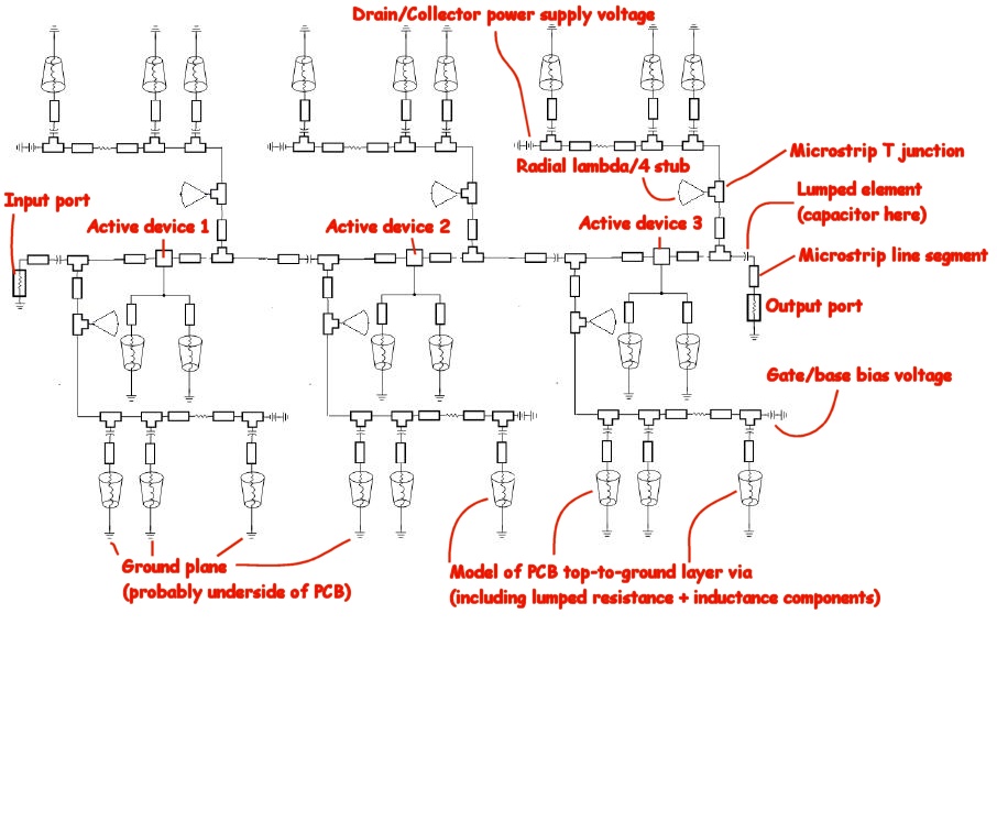
Heya electronicman - I present one annotated picture:
The circuit as drawn is a typical halfway-between-a-schematic-and-layout circuit topology often seen in RF circuit design. If I had to guess, it has a decidedly "Agilent ADS" feel about it. Here, *every* copper feature is explicitly noted/drawn - such as the T-pieces used to form a junction between three conductors belonging to the same 'net'. As you've pointed out, it's a three stage amplifier - where each stage has individually adjustable/configured bias & power supply voltages.
The radial stubs are used to present low impedance 'shunts' to the frequency of operation, thereby aiding the decoupling of the AC and DC current paths. All vias are explicitly modelled (via a substrate and geometry specification - not shown).
It's a very generic design, and you'd need to know a lot more about the specifics of the active devices before you could create a functional layout from it.
Good luck!
Thanks in advance thylacine1975 for your complete reply
at first I want to simulate the proposed LNA circuit of this conference paper:
**broken link removed**
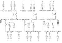
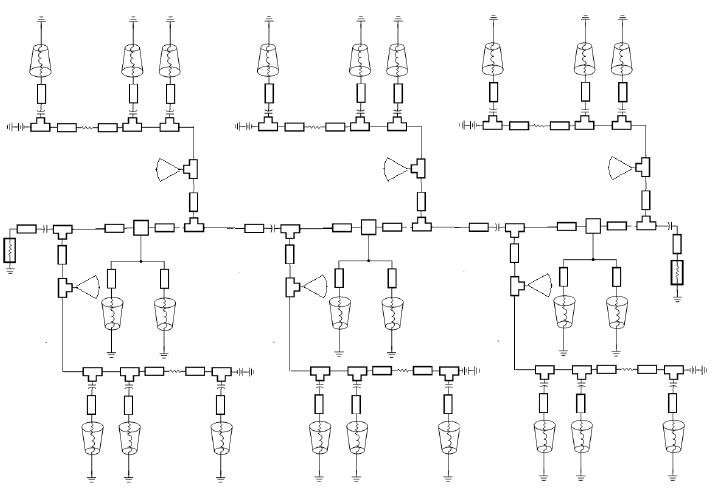
the circuit schematic of proposed LNA is this, but it isnt clear parameters value at paper, can you help me how it is possible for me to find the value of parameters?
As thylacine1975 said, that's pretty generic. It is more or less a basic diagram for every single microwave amplifier, so there is not much else to say unless you provide more data.
This site uses cookies to help personalise content, tailor your experience and to keep you logged in if you register.
By continuing to use this site, you are consenting to our use of cookies.