Continue to Site

Welcome to EDAboard.com

Welcome to our site! EDAboard.com is an international Electronics Discussion Forum focused on EDA software, circuits, schematics, books, theory, papers, asic, pld, 8051, DSP, Network, RF, Analog Design, PCB, Service Manuals... and a whole lot more! To participate you need to register. Registration is free. Click here to register now.

i-v Characteristics of bjt

Status
Not open for further replies.

aina_k

Newbie level 4
Joined
Jan 17, 2012
Messages
5
Helped
0
Reputation
0
Reaction score
0
Trophy points
1,281
Location
pAKISTAN
Activity points
1,323
I am working on simulation of SiC bjt and simulating i-v characteristics of common emitter bjt. I have applied 2.5 volts at base and 25 volts at collector . My problem is that my curve dosen't start from zero i.e, it start from 0.6 volts. I donot understand the reason. Can anybody plz tell me the reason . I also have attached My Curve image so you people can easily understand the nature of my problem
 

My problem is that my curve dosen't start from zero i.e, it start from 0.6 volts. I donot understand the reason.

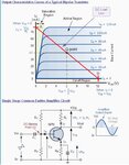
It is not a "problem". In contrary, the diagram shows the correct behaviour of a BJT. What happens for Vce=0? The B-C junction is forward biased and there is a current through the collector node, that is opposite to the "normal" Ic direction. As a consequence, the Ic-Vce curve does not cross the origin.
(However, this property cannot be seen in normal data sheets).
Remark: I am a bit surprised about the mentioned base voltage (2.5 volts).
 

Yup VcE=0. but i want to know the reason why the bjt showing this kind of behaviour in the curve as you have said in all datasheet and in books the i-v curves have showm ideal behaviour? I just want to know the reason
 

Your input details about circuit is incomplete. Please tell us, what is the emitter/collector loading, This must be npn transistor.
VCE can reach to 0 volts, but reverse current shows some reactive loading at the BJT ends.
 

Yup VcE=0. but i want to know the reason why the bjt showing this kind of behaviour in the curve as you have said in all datasheet and in books the i-v curves have showm ideal behaviour? I just want to know the reason

I think, I have explained the reason in posting#2.
This negative current (Ic) in the µA range for Vce=0 is not visible in data sheets because of the scaling More than that, for "normal" (classical) BJT applications this property is not very important.
 

Hi LvW, good Morning.
I am understanding the point you have given. But the same time my analysis tells, VCE near to 0 is very common with overdrive base voltage. That time Ic current might have very less offcourse but positive without doubt. If it is negative, Vce polarity should have changed.
 

Hi,

I am with LvW :)

If Vce is forced to be zero and there is a bias at the base-emitter (NPN transistor) then there would be a 'tiny' current flowing from base to collector (actually to ground) which is added to the load current. This current decreases in value when Vce is a bit higher than zero volt till it reaches zero value at some positive Vce voltage.

Kerim
 

'tiny' current flowing from base to collector (actually to ground) which is added to the load current.
No still not clear. Are you telling Ibc is dominated over Ice near VCE~0.
 

No still not clear. Are you telling Ibc is dominated over Ice near VCE~0.

If Vce=0 there can be no current between C and E because of the short circuit. There are only 2 currents possible: Ibe and Ibc.
 

If Vce=0 there can be no current between C and E because of the short circuit. There are only 2 currents possible: Ibe and Ibc.
I was thinking about the case where VCE is zero with zero current. I found this is not the normal case, instead we have some reactive loading at the Emitter end.
Am I correct?
 

Do you mean that there is also minority carrier current that is visible in the Characteristics Curve???

---------- Post added at 17:14 ---------- Previous post was at 17:07 ----------

what is meant by reactive loading?
 

Hi aina_k, I am interested to see your simulation setup of the your circuit.
 

BJT ICvs VCE curve.JPG
Hi Sorry, I found the above graph, same as posted by original owner of this post.
I understood the point, that the collector current becomes negative under cutoff region. not under active or saturation region.
That means when emitter and collector regions are reverse biased.
Minority carrier current that is visible in the Characteristics Curve???
This is right. This negative current shows minority carrier current only under cutoff region.
 

Status
Not open for further replies.

Part and Inventory Search

Welcome to EDABoard.com

Sponsor

Back
Top