Continue to Site

Welcome to EDAboard.com

Welcome to our site! EDAboard.com is an international Electronics Discussion Forum focused on EDA software, circuits, schematics, books, theory, papers, asic, pld, 8051, DSP, Network, RF, Analog Design, PCB, Service Manuals... and a whole lot more! To participate you need to register. Registration is free. Click here to register now.

soft connection warning: need clarification!

Status
Not open for further replies.

Braski

Full Member level 3
Joined
Dec 22, 2009
Messages
154
Helped
32
Reputation
64
Reaction score
28
Trophy points
1,308
Location
Florence (ITALY)
Activity points
2,384
I know what is soft connection. However, i still have one problem, and i don't know if i am doing right

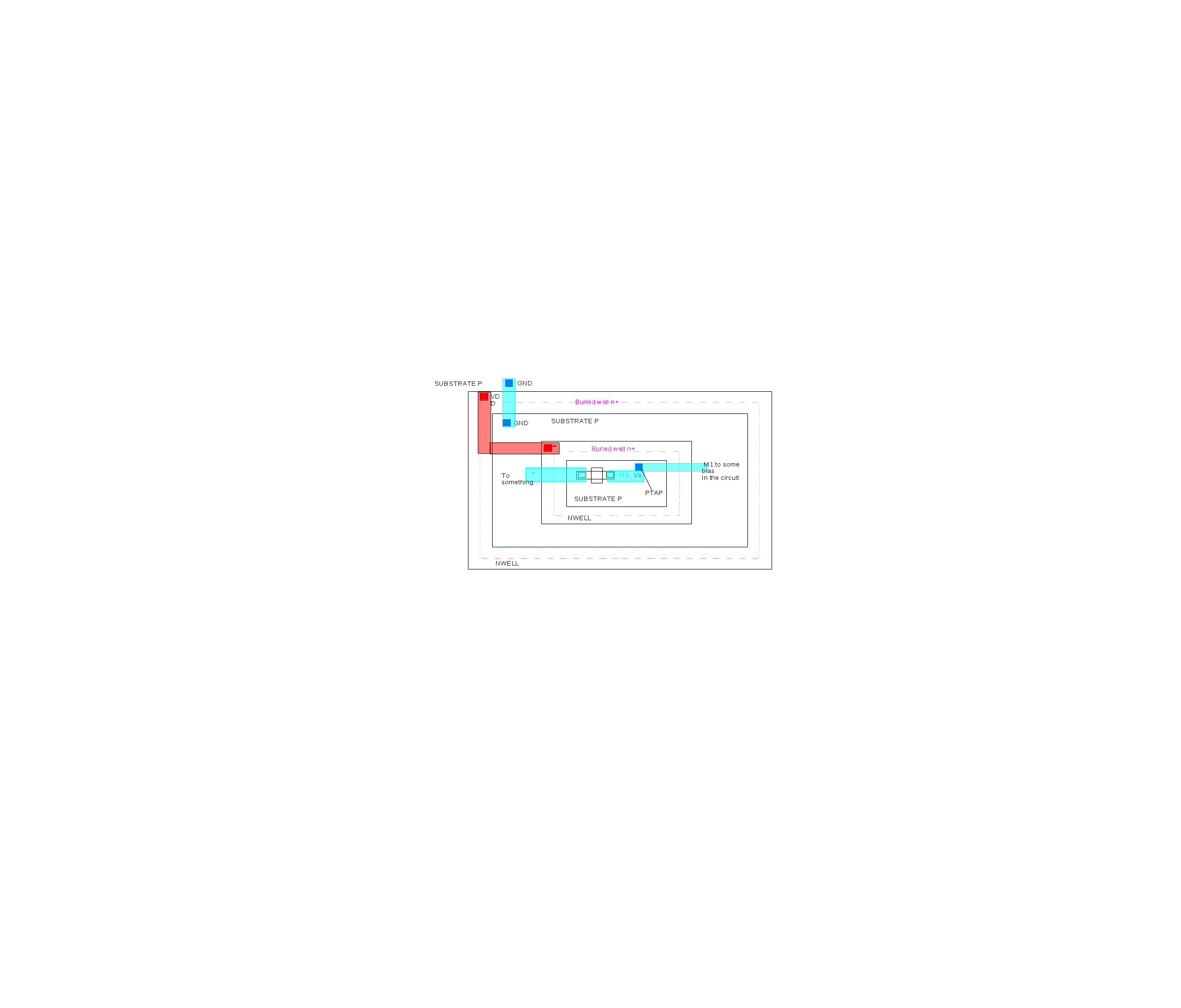
i have a buried n+ layer in my process.

i have some nmos with b-s connection, instead of bulk to ground.

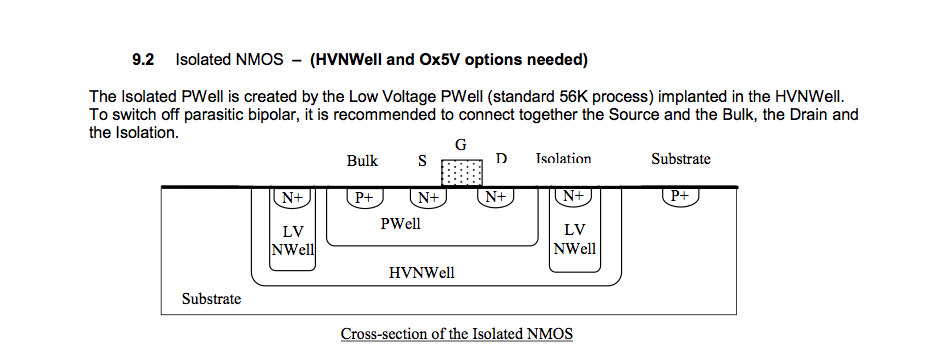
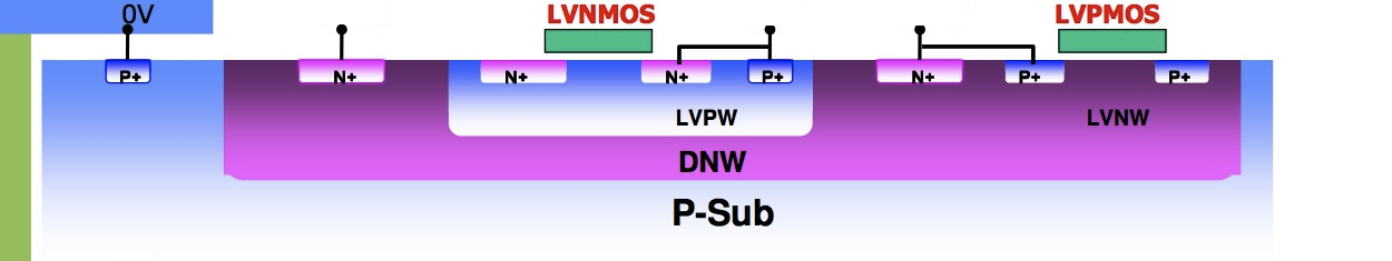
as far as i know, i need to put these nmos in an isolated pwell. To do it, i draw a nwell ring, with a buried n+ to close from below. I can put the MOS herein and put this pwell wherever i need.

After completion of my circuit, i need to make a guard nwell ring around the whole circuit, with its buried. The foundry needs it.

I put my pwell nmos inside the ring. The buried layers become ONE layers, and the pwell is still isolated in my opinion. BUT calibre lvs give me SOFT CONNECTION WARNING between gnd! and the source net of the isolated nmos.

WHY??? am i missing something?

if you need i wil post a drawing
 
Last edited:

i have some nmos with b-s connection, instead of bulk to ground.
... the pwell is still isolated in my opinion.
The source of this NMOS -- connected to its bulk, as you say -- must of course have a defined potential (more positive than ground). Otherwise calibre detects a soft connection to ground via the nwell, if this nwell is not connected to a higher potential. This underlying buried nwell via its n+ ring should be connected to VDD.

if you need i wil post a drawing
Would be nice, anyway, incl. recognizable potential connections.
 
  • Like
Reactions: Braski

    Braski

    Points: 2
    Helpful Answer Positive Rating
The source of this NMOS -- connected to its bulk, as you say -- must of course have a defined potential (more positive than ground). Otherwise calibre detects a soft connection to ground via the nwell, if this nwell is not connected to a higher potential. This underlying buried nwell via its n+ ring should be connected to VDD.

the source of the NMOS connected to its bulk has obvioulsy a defined potential (it is connected to some other node in the circuit), more positive than ground. The nwell is connected to vdd. The buried nwell is connected to vdd through the surrounding nwell (around the circuit). I'll post a drawing later, when i have 10 minutes.

I think all the connections are right...

---------- Post added at 09:46 ---------- Previous post was at 09:03 ----------

here is the image:


it should be quite clear... the gate connection is not shown for simplicity. the source is connected via ptap to the sub p in the resulting pwell. the ptap is also connected to some node in the circuit. all the nwells are connected to vdd. the buried well layers merge into 1 polygon, connected to vdd via the two ntaps.

is there some issue or the calibre warning can be ignored?
 

I think all the connections are right...

Yes, but ... your NMOS is in a region called SUBSTRATE P , hence C@libre obviously establishes a soft connection.

Instead of in SUBSTRATE P , the NMOS should sit in a PWELL, I think.

On p-substrates, its normal to have isolated NMOS transistors in a pwell sitting in an nwell.
 
  • Like
Reactions: Braski

    Braski

    Points: 2
    Helpful Answer Positive Rating
Yes, but ... your NMOS is in a region called SUBSTRATE P , hence C@libre obviously establishes a soft connection.

Instead of in SUBSTRATE P , the NMOS should sit in a PWELL, I think.

On p-substrates, its normal to have isolated NMOS transistors in a pwell sitting in an nwell.

i called it SUBSTRATE P to point out that no layer was added in this region. maybe i should add a pwell layer just to let calibre know it? i checked however the extracted netlist,which shows that the bulk connection is resolved to what i want. besides, no erc or softcheck error are raised, only a warning. i can argue that it's ok? i'll try the pwell layer, howeve.
 

i can-t understand why it is necessary. the nwell layer of my tech contacts the buried n+ creating a pwell by itself. the nwell is connected to vdd.

---------- Post added at 14:28 ---------- Previous post was at 14:19 ----------

i would like to add:

from the DK
"LVPWELL is drawn without drawing any layer as it is generated automatically
(complementary to any n-type well) by merging flow"

thus, i think that i don-t need to add any layer. the substrate portion isolated by the inner nwell and th eburied n layer constitutes automatically an isolated pwell.
 

the nwell layer of my tech contacts the buried n+ creating a pwell by itself.
Ok, if your isolated NMOS bulk actually is totally isolated from your p-substrate by a buried N+ layer & N+ ring, a further pwell implant might not be necessary. Just don't give it the same name as P-SUBSTRATE, call it e.g. P_SUB1.

Some other foundries require for an isolated NMOS a pwell anyway, even for a buried N+ layer + nwell structure, s. below:

DNW ≙ buried N+ layer ; LVNW ≙ nwell (ring + N+ tap) ; LVPW ≙ pwell
 
  • Like
Reactions: Braski

    Braski

    Points: 2
    Helpful Answer Positive Rating
Status
Not open for further replies.

Part and Inventory Search

Welcome to EDABoard.com

Sponsor

Back
Top