Continue to Site

Welcome to EDAboard.com

Welcome to our site! EDAboard.com is an international Electronics Discussion Forum focused on EDA software, circuits, schematics, books, theory, papers, asic, pld, 8051, DSP, Network, RF, Analog Design, PCB, Service Manuals... and a whole lot more! To participate you need to register. Registration is free. Click here to register now.

Can someone point me to the error in the circuit design (amplifier circuit)?

Status
Not open for further replies.

scream_er

Member level 5
Joined
Feb 22, 2011
Messages
94
Helped
0
Reputation
0
Reaction score
0
Trophy points
1,286
Activity points
2,028
Hi,
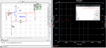
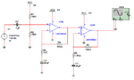
I tried simulating the attached circuit. I set my loop gain to 100x. But still I can't manage to get anything close to it. Can someone point me what I have done wrong and the solution.

Circuit 1.png

Thanks.
 

Because you are using the opamp as a dc amplifier the output contains the input offset voltage (multiplied by 100) that is contained in the opamp macro model.
By recalculating you get an input offset of Voff=1mV - 0.29 mV = 0.71 mV .
That's a quite normal value.
 

Because you are using the opamp as a dc amplifier the output contains the input offset voltage (multiplied by 100) that is contained in the opamp macro model.
By recalculating you get an input offset of 29 mV/100=0.029 mV=29 µV - a quite normal value.

Sorry, can you explain to me what you mean. In the datasheet for LM6142AI it says input offset voltage limit 1mV for 5V DC characteristic.

Attached is the circuit with AC signal. In theory I am suppose to get 2.02V. But the simulation shows 2.767. Why is it?
 

Attachments

  • AC signal circuit.png
    AC signal circuit.png
    78.8 KB · Views: 125

Forget the 29 µV. I have corrected my calculation (see above).
You have changed from double to single supply. Therefore the unexpected waveform.
 

Yup, I know I changed to single supply on purpose. But I want to know why there is a big difference in the simulation and calculation? I tried doing dual supply and it gives me a peak value of 2.7841V. So, what could be the reason?
 

Beside OA offset errors, also need to consider on the input you apply a root mean square (abbreviated rms) sinusoidal signal and on the output you measure a peak value.
U rms = U peak/1.41
20mV rms = 28.28mV peak
 

So, I get an offset of 0.7188V. So I guess there's nothing wrong with the circuit once I put an AC source. I have one more question. What indicates the offset value in datasheet ? Is the picture showing the the voltage offset value. If so why is it that the offset I am getting in simulation is not within 1mv - 2.2mv as mentioned. I am getting 0.71mv.

Datasheet.png
 

it is a bipolar input opamp, you put a large feedback resistor will introduce a large dc offset
 

Ideal operational amplifiers have zero output voltage when the differential input voltage is zero. However, real operational amplifiers do not meet this ideal goal. In most cases the data sheet will indicate the typical and the maximum value of the offset voltages.
See for this circuit
LM6144AI typical value 0.3mV, the limit value 1mV
LM6142AI typical value 0.3mV, the limit value 2.2mV
LM6144BI typical value 0.3mV, the limit value 2.5mV
LM6142BI typical value 0.3mV, the limit value 3.3mV
 

Ok, what is the meaning of limit value? Does it mean it can't go beyond that?
 

Yes, those are the maximum values permitted to a normal circuit.
 

So, I get an offset of 0.7188V. So I guess there's nothing wrong with the circuit once I put an AC source. I have one more question. What indicates the offset value in datasheet ? Is the picture showing the the voltage offset value. If so why is it that the offset I am getting in simulation is not within 1mv - 2.2mv as mentioned. I am getting 0.71mv.

View attachment 66903

Most of the data sheet values are specified with tolerances connected with a certain probability.
Your model exhibits an offest of 0.7mv - smaller than the values within the range as given in the data sheet.
So what?
This only means that the guy who has written the opamp model was of the opinion that this was a typical value.
I am sure, with a certain probability there is a hardware device that has this offset voltage.

One additional remark: If you on purpose switch to single supply you are required to add an additional circuitry for proper bias.
This subject has been discussed within this forum recently.

---------- Post added at 16:19 ---------- Previous post was at 16:13 ----------

it is a bipolar input opamp, you put a large feedback resistor will introduce a large dc offset

That's not true.
This bias current for the inv. opamp input flows (primarily) through the 10k resistor.
An opamp input dc current of - let's say - 100nA will cause an additional dc offset of 1mV.
If you are lucky (proper sign) this voltage can even reduce the offset caused by unbalanced input transistors (discussed up to now).
If not, you can use the well known bias cancellation scheme (10k resistor in front of the non-inv. input).
 

So, I get an offset of 0.7188V.
No you don't. Firstly, any OP offset voltage specification is input not output related. Secondly, the expectable output voltage is about 2.8 V, as mister_rf explained, so the input referred offset is clearly below 1 mV.

P.S.: LM6142 bias current is specified with 250 nA typically. So the 10k feedback network impedance will in fact add 2.5 mV input offset. Not a huge value, but it matters.
 
Last edited:

LM6142 bias current is specified with 250 nA typically. So the 10k feedback network impedance will in fact add 2.5 mV input offset. Not a huge value, but it matters.

So what could be the best resistor values to get a gain of 100 times?
 

As first design step, set the feed back resistor to a value suitable in terms of OP load (and possibly additional current consumption in case of a low power application). A feedback resistors of 10K is something like a standard value, a voltage divider of 10k to 100 ohm reduces the bias current related voltage drop to a neglectable quantity. Values up to 100K to 1K still keep it in a reasonable range.
 

Attached is an amplification circuit. I want to know why it cuts-off at 4V as shown in the attachment. How can I correct it?

Thanks
 

Attachments

  • 2nd Amplification.png
    2nd Amplification.png
    12.9 KB · Views: 107
  • 2nd Amplification Output.png
    2nd Amplification Output.png
    79.1 KB · Views: 111

Three options:
* Decrease the input signal
* Decrease the gain value
* Increase the supply voltage.
 

Ok, i cannot decrease the input signal. As for gain I need the voltage to be in between 0 to 5V. So if I decrease the gain then the output will be too small. So I guess the only option is to increase the supply voltage. How much do you think would be enough to get some where in between 4.5 and 5V.

Thanks.
 

You previously planned to use a rail-to-rail output OP. If you have it, you can achieve ouput voltage near to supply rails (0 to 5V).
 

Its hard to find electronics components in where I live. I couldn't find a rail to rail op-amp. I am using 5V supply, but it cuts off at 4V, does that mean the "REAL" supply voltage rail is 4V? If I change the 5V to 9V can I be able to achieve the somewhere close to 5V in the output?
 

Status
Not open for further replies.

Part and Inventory Search

Welcome to EDABoard.com

Sponsor

Back
Top