Continue to Site

Welcome to EDAboard.com

Welcome to our site! EDAboard.com is an international Electronics Discussion Forum focused on EDA software, circuits, schematics, books, theory, papers, asic, pld, 8051, DSP, Network, RF, Analog Design, PCB, Service Manuals... and a whole lot more! To participate you need to register. Registration is free. Click here to register now.

[SOLVED] How dense could a manual solderer solder?

Status
Not open for further replies.

mmitchell

Advanced Member level 4
Joined
Dec 3, 2011
Messages
107
Helped
0
Reputation
0
Reaction score
0
Trophy points
1,296
Activity points
2,203
Hi,

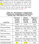
In IPC-7351, table 3-4 to table 3-14 contain the defined “courtyard excess” for placement density level A, B and C. According to Note 3 on page 1, definitions in this IPC-7351 standard are for reflow soldering.
Courtyard_soldering.png

In prototyping however, can I ask a solderer to solder level C spacing board?

Take capacitors and resistors for example. By table 3-6, “courtyard excess”

  • Level C: 0.1mm
  • Level B: 0.15mm
  • Level A: 0.20mm

If one chooses level C, the minimum pad spacing between different components (capacitors, resistors, and pads of other ICs) is 2x courtyard excess = 0.1 × 2 = 0.2mm = 7.874mil.

There would be solder mask between them with the usual solder mask expansion is between 0 and 5 mil. If we assume 0mil for minimum so that we get 7.874mil solder mask separating the two close pads exactly, then can it guarantee no bridging would occur? From the perspective of solder mask width this is enough; but isn’t the pad spacing too small? Can any solderer work with that?

On the other hand, if I adopt level A spacing in prototype board so that 2x courtyard excess = 0.2 × 2 = 0.4mm = 15.748mil, two times of that for level C, is it spacing large enough for solderers to handle manually?


Matt
 

I dont realy understand the content of your question. I have used all forms of the IPC-7351 format library dependant on the design complxity and have never had problems with solder bridging as long as there has been a sliver of solder resist between the pads (this is called a solder dam). What you need to do is look at manufacturers capabilities for solder dams to see what they can achieve. Also look at this thread, a picture in one of the latter posts explains the concept. If they are hand soldering a SMD device one would hope they put down solder paste and use a heat gun or use some other controlled method of applying the solder so that the correct amount is provided to make an acceptable joint with no excess solder and thus no bridging.
Dont over complicate your PCB design process, you build up your design rules and libraries so that you dont have to thi nk about these points, but can concentrate on actual PCB layout.
 
as long as there has been a sliver of solder resist between the pads (this is called a solder dam).

Another definition at **broken link removed**
solder dam A neck-down (narrowing) of a conductor that restricts the flow of molten solder. Its main purpose is to ensure that the proper amount of material remains at the solder joint that is being formed.

I think yours is correct; the other linked glossary confused necking, which is to prevent molten solder from flowing over connecting trace, with solder mask which is to prevent molten solder from joining adjacent pads.

Is this correct?

And can we use a more formal definition of "solder mask":
  1. Solder mask is a material coated over or between surface traces to prevent bridging caused by molten solder flowing.
  2. Solder dam is a sliver of solder mask situating between component pads. It is a special kind of solder mask only due to its placement and purpose, and has the same material with solder mask.
?

Also look at this thread, a picture in one of the latter posts explains the concept.
Could you provide the link?


Matt
 
Last edited:

https://www.edaboard.com/threads/231607/

---------- Post added at 15:27 ---------- Previous post was at 15:20 ----------

My definition is correct, never mind think, have a look on the internet for what is a solder dam, and as I have stated, PCB manufacturers will quote this figure so you can set your DFM rules to cater for certain manufacturers.
That definition above sounds like it is from the pre-historic days.

---------- Post added at 15:35 ---------- Previous post was at 15:27 ----------

**broken link removed**
 
You have been initially asking about courtyard excess, which is in my opinion more related to automatic assembly requirements than solder masks. Pad to pad clearance will be most critical between the pads of the same package. Minimal solder dam (I'dont know, if it's the commonly used technical term) is a design rule parameter, in high density designs, we can achieve values down to 0.05 mm (2 mils).
 
in high density designs, we can achieve values down to 0.05 mm (2 mils).

You mean pad pitch between the the same component? IPC-7351 density level C for component spacing is 0.1mm = 4mil, so this (your) 2mil min distance is for a component's pad pitch, not inter-component spacing?

Matt
 

0.05mm is a standard achievable solder dam. One of the worse components to solder are 0.5mm pitch QFPs, with these you can achieve a 0.05mm gap 0.1mm solder dam, 0.05mm gap between the pads. For most of our designs we like to keep the dams to 0.1mm, and I do use front end software to check and DFM the designs, it keeps our PCB manufacturers happy!
 
with these you can achieve a 0.05mm gap 0.1mm solder dam

marce,

0.1m should be the width of the solder dam, but what do you mean by "0.05mm gap"?

Matt
 

so this (your) 2mil min distance is for a component's pad pitch, not inter-component spacing?
I was talking about minimal solder dam. You also need solder mask enlargement of e.g. 0.05 mm, resulting in minimum pad-to-pad spacing of 0.15 mm/6 mils.

0.5 mm QFP isn't worst by the way, we also have 0.4 mm QFP. I reviewed a previous design, it used 0.2 mm pads for this package and 0.1 mm solder dam. But there was a number of failing solder joints in production.
 
FvM,

I got it, thanks for explanation. 0.4mm QFP is also the smallest pitch I have ever seen.

Matt
 

Status
Not open for further replies.

Part and Inventory Search

Welcome to EDABoard.com

Sponsor

Back
Top