Continue to Site

Welcome to EDAboard.com

Welcome to our site! EDAboard.com is an international Electronics Discussion Forum focused on EDA software, circuits, schematics, books, theory, papers, asic, pld, 8051, DSP, Network, RF, Analog Design, PCB, Service Manuals... and a whole lot more! To participate you need to register. Registration is free. Click here to register now.

Whould this circuit work? (Driving p-Channel MOSFET)

Status
Not open for further replies.

hkBattousai

Advanced Member level 4
Joined
Jun 16, 2007
Messages
118
Helped
5
Reputation
10
Reaction score
1
Trophy points
1,298
Location
Turkey
Activity points
2,182
**broken link removed**

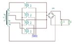
I'm designing a power supply. Main power source is a transformer. The transformer has multiple taps; 9V, 15V, 24V, 36V, 48V. For obtaining as much efficiency as possible, a control circuit is monitoring the output voltage of the power supply and switching between transformer taps according to it.

v(t): Rectified voltage of a transformer by a bridge rectifier
Load: Filter and regulator stage

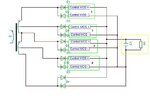
Actually, there will be 5 of this circuit in the picture, each for a different transformer tap. And they all will be connected to the same load (filter & regulator).

My question is,
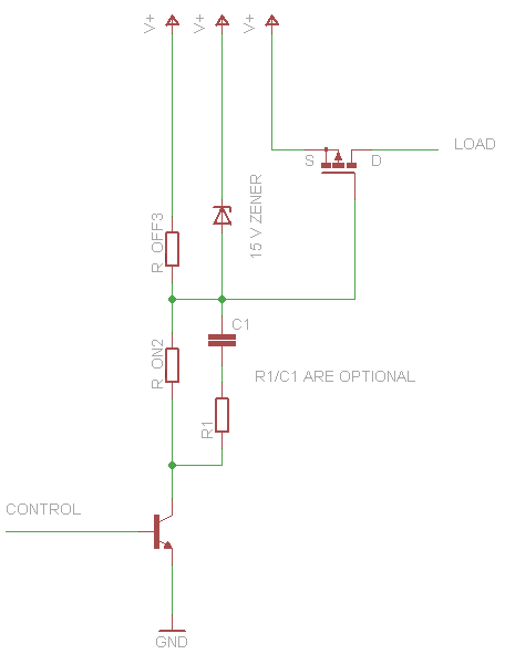
Would this circuit run alright?
I'm not very familier with MOSFETs, so I'm not sure if I'm driving IRF9530 in a correct way. I need you to confirm my design, or suggest me some corrections on it.
 

I think it can work but only if you connect the output filter capacitor of the bridge in the input Vt because you need to have a voltage in the input that keeps a min level so that the mosfet stays on (like >5v).
you also need to add a diode in the output (drain) of IRF9530 because if I understand correctly all the drains will be tied together so when a mosfet connected to a higher voltage turns on it will provide to the drains of the other mosfets a higher voltage compared to the source and the mosfet diode will conduct (drain>source voltage).
You need diodes with the cathode in the load side and the anodes connected to the drains and then connect the cathodes together as output.

Alex
 
No, this schematics don’t work on the ac lines.
What you want to do is to emulate an analog switch, which is a paralleled pair of MOSFETs, one N-channel other P-channel, which allows current to flow bi-directionally.
See some details here:
https://www.vishay.com/docs/81225/ssrvo126.pdf
 
He is not connecting the transformer tap directly, he said
v(t): Rectified voltage of a transformer by a bridge rectifier
so the input to the mosfet source is already full wave DC so if he also adds a bridge capacitor there it should work

Alex
 
He is not connecting the transformer tap directly, he said

so the input to the mosfet source is already full wave DC so if he also adds a bridge capacitor there it should work

Alex

Yes, very good idea.
Would it cause any problem like overshoots or spikes while switching between transformer taps?
 

A more practical approach for this application using standard relays, the tap point = rectifier bridge input to be disconnected by relays and connected to the new terminal.
 

Attachments

  • Tap control.JPG
    Tap control.JPG
    36.2 KB · Views: 109
A more practical approach for this application using standard relays, the tap point = rectifier bridge input to be disconnected by relays and connected to the new terminal.

From the very start I insisted on making a completely solid state design. But looks like the hardware design challenges are pushing me to use standard relays once again.
I wish those SSRs weren't that much expensive...
 

He is not connecting the transformer tap directly, he said
"v(t): Rectified voltage of a transformer by a bridge rectifier"
Yes, the information is also shown in the first post by writing abs(sin()), which has been apparently overlooked.
so the input to the mosfet source is already full wave DC so if he also adds a bridge capacitor there it should work
A filter capacitor before the MOSFET switch(es) would charge the capacitors of the inactive channels by the MOSFET reverse diode. The original circuit has however a weakness by the 20 V series Z-diode, because the switch will only conduct at higher input voltages. An the gate voltage will still exceed the maximum rating with 50 Vpeak input. You should better use a voltage limiting diode across the gate and preferably a constant current driver stage.

I agree however with mister_rf, that mechanical relays are probably the more reasonable option.
 
A solid state device on DC line need to control 2 lines simultaneous in pairs, like this :
 

Attachments

  • DC Tap control.JPG
    DC Tap control.JPG
    53.3 KB · Views: 83

A solid state device on DC line need to control 2 lines simultaneous in pairs.
Seems to be a promising approach, using NMOS for + and PMOS for - branches, needing only two isolated multi-channel gate drive circuits.
 
A filter capacitor before the MOSFET switch(es) would charge the capacitors of the inactive channels by the MOSFET reverse diode

What you describe can only happen if a mosfet connected to a higher voltage turns on but I have mentioned in my first answer (#2) that he should also use diodes connected to the drains in the reverse polarity of the substrate diode to prevent that.

Alex
 
What you describe can only happen if a mosfet connected to a higher voltage turns on but I have mentioned in my first answer (#2) that he should also use diodes connected to the drains in the reverse polarity of the substrate diode to prevent that.

Alex
Actually there are diodes in the original design, but I simplified the circuit while drawing this picture.
 

Sorry to come late to this discussion. I tried the circuit in post #1 a few years ago. In fact, there are several variations that can be devised. One sage person asked, what happens if the zener fails shorted?

I revised the circuit to that shown here to avoid destroying the mosfet gate by that condition:
23_1314966353.png


Another person suggested adding R1/C1 as a "speed up". I used values of 150Ω and 470 pF and got noticeably faster turn on, but that part is optional.

John
 
what happens if the zener fails shorted?
1. Why it should? 2. No problem.
Another person suggested adding R1/C1 as a "speed up"
As far as I understand, switching 50 Hz AC voltage won't need speed up.

As possible problem, also regarding speed, is the dimensioning of R2 and R3. Basically, the MOSFET threshold voltage involves a minimum input voltage to activate the switch. R2 and R form a divider, that further increases this threshold unless R2 << R3. R2 has a minimum value due to Z-diode and resistor power dissipation. This results in a rather large value for R3 and thus slow turn-off.

To overcome this problem, I suggested to supplement the NPN transistor to a constant current source.
 
Failing shorted is a common way zener diodes fail.
First, there has been a misunderstanding. I understood the comment about z-diode failure related to second circuit. For the first circuit, short of the Z-diode would be in fact bad, but you can also damage the MOSFET with the z-diode still intact.

Generally, Z-diodes don't fail accidentally, they fail by overload. Even in the first circuit, there's no particular risk of z-diode overload.
 
Last edited:
Status
Not open for further replies.

Similar threads

Part and Inventory Search

Welcome to EDABoard.com

Sponsor

Back
Top