Continue to Site

Welcome to EDAboard.com

Welcome to our site! EDAboard.com is an international Electronics Discussion Forum focused on EDA software, circuits, schematics, books, theory, papers, asic, pld, 8051, DSP, Network, RF, Analog Design, PCB, Service Manuals... and a whole lot more! To participate you need to register. Registration is free. Click here to register now.

help on ADC accuracy!

Status
Not open for further replies.

overmars

Member level 3
Joined
Sep 11, 2006
Messages
65
Helped
5
Reputation
10
Reaction score
1
Trophy points
1,288
Activity points
1,754
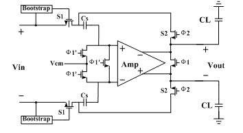
I designed a 14-bit 50Msps pipelined ADC, I used fully differential flip-around THA, and the virtual ground voltage set to Vcm as shown in the figure. If I vary Vcm, the whole accuracy of my ADC varied accordingly. But ref to the thoery, the Vcm will not affect the conversion accuracy. So where's the problem ?

The pipeline is a 3.5bit of first stage , and 8*1.5bit/stage with final 3-bit of last stage.

When doing post-layout simulation, the offset seems to be 10LSB and gain error 5LSB which is out of requirement. Then I vary the reference and set the positive and negative ref externally, but the offset and gain error do not reduce. Why is that?

---------- Post added at 10:37 ---------- Previous post was at 10:34 ----------

figure
18_1312105043.png
 

I guess we need a few more pieces of the puzzle:
- why are you showing us the THA, have you already narrowed down the problem to it?
- if so does the problem exist in pre-layout simulation?
- if I had to take a wild guess, assuming the problem is the THA and only post-layout, I would look at uneven injection of a digital line to one of the virtual grounds...

I would help breaking your layout in diff op amp and everything else (switches) and see if you can isolate the problem to either block

In summary, you should provide more details
 

Can you tell me what detailed part I shall upload here?

I'm sorry, it is not the problem due to THA but first pipeline stage instead. The virtual ground node of first stage is set to Vcm. Theoretically the matching of MDAC capacitor is the main contributor to the nonlinearity. But in pre-simulation, there is no matching parameter involved.

If the virtual ground Vcm varies, the final accuracy of ADC varies. This problem has nothing to do with the layout as this is a pre-simulation. So I wonder if the reason is related to the voltage coefficient of PIP capacitors.

If I only extract the first stage from layout and running simulation, the final ADC accuracy is much worse than full extraction results. I guess this is due to asymmetrical layout of some of the diff signal line.

Another puzzle is that when varying the positive and negative reference bias, the final offset and gain error do not getting better in post-layout simulation.

please help!
 

additional nonlinearity can be sourced from bootstrapped switch. Settling time of higher and lower switches will depend from Vcm. At 14-bit accuracy it might be esential.
 

I think this is the fully diff structure, the switches which connect to Vcm has the same Vds and Vgs, the settling seems to be the same. Please correct me!

Could you explain more specific why and which one is the higher and lower settling switch?

Thank you!
 
Last edited:

Vds_S1_high, Vds_S1_low are approximately the same (i.e. ~0V, when settled), but Vdb, Vsb are different (Vdb_S1_high=Vin+ =/= Vdb_S1_low=Vin-) and, therefore Vth_S1_high and Vth_S1_low are different. Fot big positive signals switch S1_high will have much more Ron than S1_low, leading to increasing of settling time.
 
Here the Vcm i mean the virtual ground node of the OTA, not the input common mode signal. u can see that the Vcm connects to the bottom-plate sampling switch. Even the settling of input switches S1 is different, how does it relate to the virtual ground voltage ?
the fact is that when i equal the virtual ground voltage Vcm to input common mode, here the input common-mode is 1.6V, the overall offset increases. If decrease this voltage to 1.2V, the input common-mode maintains as 1.6V, the overall offset decrease by serval LSB. How can u explain this?
Thank you for your further reply.
 

Vcm influences on Ron of swithches S2_high, S2_low as bigger as positive OA output voltage swing, and Vcm themself are higher. Vcm should be chosen from criteria not only optimal linear OA behaviour, but desirable settling time (~Ron of switches S1, S2) also.
 
Can u tell me how to calculate the optimal virtual ground voltage?
 

because you use NMOS switches only, from lowering Ron target, the lower Vcm the better. But first of all Vcm have to provide transfering of nondistorted signal. Therefore voltage swing at the S/H output (assume that Vcm_in =Vcm_out=Vcm) plus say 20% margin will define Vcm (i.e. 1.2x(Vswing/2)) approximately. Then you have to define which size of S1, S2 switches can provide necessary maximum worst case Ron (i.e. Ron_max < Ron_target) with your concreate bootstrep circuit. If it isn't possibble with any NMOS sizes, then investigate possibility to reduce swing, look for another architectural solutions,... Circuitry of OA then have to be designed to provide a non saturated output in the (0.1xVswing...1.1xVswing) range.
 
Status
Not open for further replies.

Part and Inventory Search

Welcome to EDABoard.com

Sponsor

Back
Top