Continue to Site

Welcome to EDAboard.com

Welcome to our site! EDAboard.com is an international Electronics Discussion Forum focused on EDA software, circuits, schematics, books, theory, papers, asic, pld, 8051, DSP, Network, RF, Analog Design, PCB, Service Manuals... and a whole lot more! To participate you need to register. Registration is free. Click here to register now.

how to eliminate ringing in single phase inverter

Status
Not open for further replies.

thelukuntla

Junior Member level 1
Joined
Sep 2, 2008
Messages
16
Helped
0
Reputation
0
Reaction score
0
Trophy points
1,281
Location
New delhi
Activity points
1,411
hi

I am making a single-phase inverter with a dc-dc boost converter for my project and with an aim to make it to 1 kw rating and 230 V, 50Hz rms using dc power supply in the lab with 175V and 10A supply.

I followed guidelines given in 6N136, IR2110 and AN-978 , DT97-3 datasheets and kept Rgon=15 Ω and Rgoff=8.2Ω using anti-parallel diode across Rgon and made individual driver circuits for all switches.
MOSPETS used : STW20NK50Z
Switching frequency: 10KHz
PWM pattern: Sine

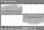
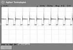
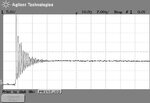
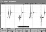
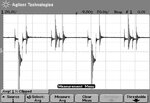
Initially i made the inverter circuit and tested with low input dc voltage around 12V and measured output of inverter circuit i found still ringing effect and switching noise more than double the input dc voltage. some screen shots of output waveform are given as attachments.
I made separate high side drivers for all MOSFETS (4 no.s) of single-phase inverter. Optocoupler and IR2110 driver portion of the circuit is on PCB and rest inverter portion of switches are mounted on separate board, connection between driver output to gate and source terminals of MOSFETS done by using wires of around 10-15 cms in length.I kept bootstrap capacitors with 4.7μF and 10 μF for high side and low side of IR2110.
As my power circuit ground is different from driver circuit ground, so i kept 4 no. separate high side drivers to drive each MOSFET and using only high side part of the IR2110 IC.

let me know where i am doing mistakes.

Thanks in advance.

Chandra Shekar
 

Attachments

  • PRINT_00.JPG
    PRINT_00.JPG
    29.5 KB · Views: 127
  • PRINT_01.JPG
    PRINT_01.JPG
    21 KB · Views: 120
  • PRINT_03.JPG
    PRINT_03.JPG
    21.4 KB · Views: 126
  • Driver ckt_IR2110.pdf
    41.3 KB · Views: 140

The schematic misses a VSS connection. I don't see an indication however, that the ringing is driver related. Ringing considerably above the bus voltage shouldn't happen in a reasonable inverter layout, because it's clamped by the output diodes.

We would need to see aditional waveforms, e.g. HS and LS gate voltages, bus voltage to understand more.
 
We would need to see the complete schematic for the power circuits and driver connections - the first 3 rules of power electronics are 1) layout, 2) layout & 3) layout, it appears you may not have enough de-coupling on your power circuits and the layout may be too open - i.e. too much inductive loop areas and bus caps too far away (if there are any) any photo's would be very helpful too.
 
  • Like
Reactions: FvM

    FvM

    Points: 2
    Helpful Answer Positive Rating
Thanks for the response and finding mistake in driver layout. Whether my driver ckt layout is valid one for high side MOSFET/switch,and i have doubt in Vs and COM connection of my driver ckt layout. please check
 

Attachments

  • PRINT_01_Vds_drain-source voltage_MOSFET1.JPG
    PRINT_01_Vds_drain-source voltage_MOSFET1.JPG
    28.4 KB · Views: 140
  • PRINT_02_Vgs_Gate-source voltage_MOSFET1.JPG
    PRINT_02_Vgs_Gate-source voltage_MOSFET1.JPG
    28.2 KB · Views: 142

As FvM said, there shouldn't be any ringing above the bus supply. If you have significant lead inductance, then it can overshoot higher, but it should be limited to twice the bus voltage. But you're seeing even more than that, so there's something very wrong. I would first suspect the layout of the bridge itself. Use short and wide connections between the bridge and the DC bus capacitance. For bus capacitors, use a combination of large electrolytics and smaller, but faster film capacitors. The long leads from your gate driver are probably also an issue, especially if they form loops. Try twisting gate/source pairs tightly together.

Are those waveforms taken with a load?
 

referring to your gate drive schematic, for low side devices you can usethe low side half of the 2110, you need to study the data sheet carefully...!
 

hi

As my power circuit ground is different from driver circuit ground, so i kept 4 no. separate high side drivers to drive each MOSFET and using only high side part of the IR2110 IC.

Actually there is a dc-dc boost circuit between dc supply and inverter, due to which low side switch potential w.r.t dc supply (-ve dc rail) are different means not at zero potential, it equivalent to floating voltage. So i am using only high side part of IR2110 IC, and made 4 such circuits to each MOSFETs.
My queries are:
1. between Vcc and COM, cap is required or not.
2. as Mr. FvM pointed, whether cap is needed between Vdd and Vss.
3. whether Vs and COM can be connected.
4. whether Vss, Vs and COM can be connected (in high side config.).

Thanks in advance
 

Attachments

  • Driver ckt_IR2110.pdf
    41.3 KB · Views: 129

Your explanantion doesn't correspond to the circuit diagram, which shows a common ground of IR2210 logic side and DC bus. Actually, IR2110 would never work with a floating ground. You have been quoting the respective IRF applications notes, and this point should be clear from carefully reading them.

I initially understood your motivation for not using the IR2210 low side driver in the expected high noise level. I wonder however, if this is a well-founded decision. The low side driver allows some ground potential differences between logic (VSS) and output (COM) side. Clearly, Vcc must not swing below Vss. But this also not permitted for VB. Just look at Figure 10. IR2110 Parasitic Diode Structure in DT97-3. Floating ground is not permitted, because a return path for the control current between input logic and high side must exist.

My assumption is, that using the IR2110 low side driver for the low side switches involves similar restrictions as using high side only. As I already mentioned, VSS must be connected in any case. I'm not sure, if it's necessary to supply the unused low side drivers (you could use a single high side driver chip in this case as well), but it shouldn't do any harm.

As I also stated, I don't see an indication for driver related problems at present (except for missing VSS connection). It may be the case, that overlapping gate drives are causing shoot-through, or that an unsuitable gate signal wiring results in ringing gate voltages and respective oscillations. But even in this case, you shouldn't get output voltages swinging widely out of the DC bus range. This is either a problem of bad power circuit layout or incorrect probing.
 

I have connected Vss to COM, and i tested the whole circuit, it's drawing huge current even at lower voltages also. What might be the reason, the modified driver circuit is attached.
 

Attachments

  • Driver ckt_IR2110.pdf
    48 KB · Views: 123

I don't see anything really wrong with the schematic at a glance. You should include the load and the rest of the inverter circuit (you're using a half bridge, right?) though. You'll have to post some waveforms or something for us to be able to help.
 

where does the drain of the fet go to? +Vcc? the whole circuit would be good - otherwise impossible to answer your question
 

Status
Not open for further replies.

Part and Inventory Search

Welcome to EDABoard.com

Sponsor

Back
Top