Continue to Site

Welcome to EDAboard.com

Welcome to our site! EDAboard.com is an international Electronics Discussion Forum focused on EDA software, circuits, schematics, books, theory, papers, asic, pld, 8051, DSP, Network, RF, Analog Design, PCB, Service Manuals... and a whole lot more! To participate you need to register. Registration is free. Click here to register now.

clamp diodes in mosfet

Status
Not open for further replies.

anandkamra

Newbie level 4
Joined
Jan 4, 2010
Messages
6
Helped
0
Reputation
0
Reaction score
0
Trophy points
1,281
Activity points
1,330
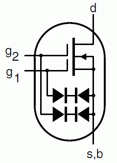
Ques1 -->How clamp diode at gate of mosfet prevent accumulation of charge at gate?
Ques2-->How diode betweent drain and source helpful or what is its purpose ? Is it also use for some prevention? How it prevent mosfet?
 

Ques2-->How diode betweent drain and source helpful or what is its purpose ? Is it also use for some prevention? How it prevent mosfet?

It does not necessarily means to provide any protection. This diode came in picture due to inherent internal structure of FET. In some of circuit topologies this diode helps to have a freewheel path for the current while driving a inductive load and we can say it is protecting the FET for high transient voltage in these topologies.
 

MOSFET aren't generally provided with a clamp diode at the gate. They may possibly have ESD protection. Which transistor type you are referring to?

All power MOSFET have bulk (substrate) connected to source and a built-in drain-to-substrate diode, necessary by technology. It's not provided for a particular purpose, but must be considered in circuit design. Sometimes it's helpful. In a standard MOSFET, the diode has slow recovery, which is mostly unwanted. Some transistor types are speeding up the diode by special means.
 
Diodes on the input are to protect the oxide layer from damage ( punch through ). The body diode is an unavoidable parasitic.
 

Actually I am studying sedra smith.
on page 259- 260, topic 4.2.7 B reakdown and Input Protection
To prevent the accumulation of static charge on the gate capacitor of a MOSFET, gate protection
devices are usually included at the input terminals of MOS integrated circuits.
The protection mechanism invariably makes use of clamping diodes.,
This I want to know how this happens? how this clamping diode is connected? how prevention occurs fromaccumualation of charge ?
Please explain me?


Also --> is it antena effect?

yes I have also see wikipedia but i want to know if we connect cathode to gate of mosfet anode to ground or VSS i.e in reverse then how accumulate charge from gate discharges ?(or if we connect diode in opposite way then signal at gate will be grounded. )
 
Last edited:

The term "accumulation of charge at gate" is rather vague in my opinion. Adding "static" clarifies, that you are talking about common ESD protection. I keep my opinion, that MOSFET don't generally have gate protection circuits. If they have it, anti-series connected (back-to-back) zener diodes can be expected, as in the below (dual gate) MOSFET.

1_1305097208.gif
 

yes , Static accumulation of charge at gate
 

Status
Not open for further replies.

Similar threads

Part and Inventory Search

Welcome to EDABoard.com

Sponsor

Back
Top