Continue to Site

Welcome to EDAboard.com

Welcome to our site! EDAboard.com is an international Electronics Discussion Forum focused on EDA software, circuits, schematics, books, theory, papers, asic, pld, 8051, DSP, Network, RF, Analog Design, PCB, Service Manuals... and a whole lot more! To participate you need to register. Registration is free. Click here to register now.

Minimum scribe line distance to active devices?

Status
Not open for further replies.

banvetor

Junior Member level 1
Joined
Jun 20, 2009
Messages
15
Helped
0
Reputation
0
Reaction score
0
Trophy points
1,281
Location
Brazil
Activity points
1,440
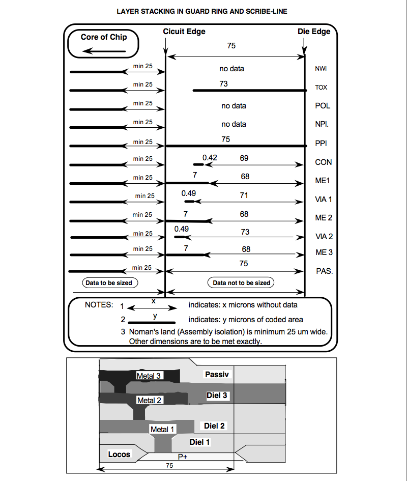
Hi, I'm finishing a design on AMS H35B4 tech, but my chip does not have PADs on all sides...

I'm not sure if I indeed need to put the scribe line on my design, of if just the min. width MET1 path is enough... in any case, my real question is: what is the minimum distance I should put my circuit from this line?

Surprisingly, I could not find this information on the design docs!

Thanks,
Leo.
 

Please check your process design rule document. Between scribe line and internal circuit, you still need seal ring. Usually for seal ring to internal circuit, it needs 15um+ buffer region.
 

Hi Leo,

Thanks for the help. On the design docs, the seal ring is described as the "SCRIBE" cell, so, although I was wrong on the terminology, we are talking about the same thing. However, the document does not seem to indicate any rule for distance between the seal ring and my circuit, maybe pointing out that I should just follow whatever standard DRC rule limits my circuit from the seal ring (MET to MET, etc)?
 

... I should just follow whatever standard DRC rule limits my circuit from the seal ring (MET to MET, etc)?
I think this is not enough. Below see the necessary distance for a 0.35µm process
from a different foundry (3 metals process):


The region between Circuit Edge and Die Edge is the scribe line. They request a min. distance of 25µm for any layer.
 

I think this is not enough. Below see the necessary distance for a 0.35µm process
from a different foundry (3 metals process):

The region between Circuit Edge and Die Edge is the scribe line. They request a min. distance of 25µm for any layer.


Hey Erik, I was thinking the same (that DRC rules were not enough), that's why I posted the question here. Anyway, it is VERY strange that AMS does not provide this info in their docs... they have a very similar pic to the one you posted, but without values for the min. circuit distance!

I e-mailed them to try to get an answer, thank-you all for the help anyway!
Leo.
 

seal ring is used to protect silicon from stress / humidity . scribe line is where wafer probe tests are dont on test circuit to study the characteristics of the fabrication process on the wafer. also some companies use the scribe line as a marker for die etching / laser cutting.
i would recommend using a seal ring to protect your chip boundary.
 

Possibly, different foundry have different descriptions.
Basically, all chips needs both seal ring that is used to isolate humidity after the chip is cut.
Usually, test device is placed in scribeline.
I agree with steadymind.
Hi Leo,

Thanks for the help. On the design docs, the seal ring is described as the "SCRIBE" cell, so, although I was wrong on the terminology, we are talking about the same thing. However, the document does not seem to indicate any rule for distance between the seal ring and my circuit, maybe pointing out that I should just follow whatever standard DRC rule limits my circuit from the seal ring (MET to MET, etc)?
 

... it is VERY strange that AMS does not provide this info in their docs...

May be your design will - at first - be produced on a multi client wafer? In such case your design must fit into a predetermined area, and the foundry provides the seal ring / scribe line.
 

May be your design will - at first - be produced on a multi client wafer? In such case your design must fit into a predetermined area, and the foundry provides the seal ring / scribe line.

Yes, indeed I'm going through Europractice MPW... but I think the docs from AMS should cover also mini-ASIC runs, so this information should in any case be there! Oh well... waiting for Europractice and AMS e-mail replies ;)
 

Status
Not open for further replies.

Part and Inventory Search

Welcome to EDABoard.com

Sponsor

Back
Top