Continue to Site

Welcome to EDAboard.com

Welcome to our site! EDAboard.com is an international Electronics Discussion Forum focused on EDA software, circuits, schematics, books, theory, papers, asic, pld, 8051, DSP, Network, RF, Analog Design, PCB, Service Manuals... and a whole lot more! To participate you need to register. Registration is free. Click here to register now.

[SOLVED] PIN DIODE NEGATIVE RESISTANCE in SPDT Switch

Status
Not open for further replies.

usman_mahfooz

Member level 2
Joined
Aug 19, 2006
Messages
50
Helped
3
Reputation
8
Reaction score
2
Trophy points
1,288
Location
PAKISTAN
Activity points
1,583
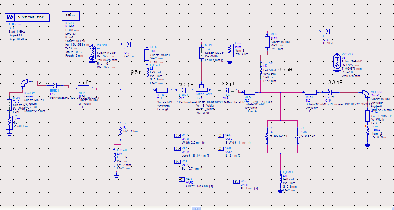
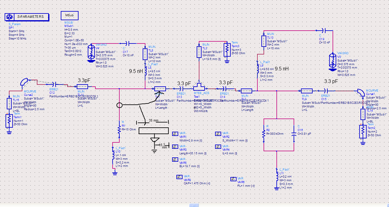
I need some help here. When measuring resistance on my pin diode in forward bias condition i am geting a reading of -9000 Mohms. It should be < 2 ohm.Circuit is of a spdt switch.
Can somebody tell me why its behaving in such a way.
NOTE:(I am not switching the bias current i-e keeping the diode in a single state)
Thanks
 
Last edited:

You are misinterpreting the results. A pin diode in forward bias is not a pure resistance. It is a complex impedance.

How are you making your measurement?
 
It maybe caused by the capacitors of your circuits. Test again. Use small range first.
 
It looks to me like you are trying to measure the resistance with a DVM, in which case you will get a nonsensical reading, could be positive or negative depending on which way round you put the leads.
The 2 ohms you refer to is the 'RF resistance' of the diode. To measure that you will need to use a network analyser at the operating frequency of your switch.
Peter
 
Thanks all for your replies. I was using the DVM .
I have another question about shunt diode switches.

When switching on an arm in SPDT switch, I get right insertion loss(Pout at the output)
but in Off state the isolation the same arm is around 1 dB (Pout nearly equal to Pin).
i am using a Microstrip substrate for the design and i have grounded the cathodes(Grounds) of diodes by soldering a normal wire b/w bottom and upper copper layer of the substrate through a drill hole(I am not using vias).
Diode is showing the proper response in the On/Off bias states but the circuit is not. Diodes are not the problem.
Any guess what could be the reason
Thank you

kyfs5ud7nlwtr5mhbtg.png
 

I would look at stray inductance in series with the diodes. It is easy to add a nano henry when using wire links.
Peter
 

Lets start off with some basics, since you started off trying to measure the microwave properties of the pin diodes with a DVM!

In your block diagram, to connect between the common port and the RF 1 port, you want to have -10 volts DC on bias pin 1, and you want perhaps 20 milliamps of current going into bias pin 2.

You show the length between the junction to the first pin diode as λ/4. That is close, but not quite exact. Because of various parasitics, and because of the phase shift thru the DC blocking capacitor, you probably want the length between junction and where the PIN diode is to be maybe 75 degrees at band center.

What pin diodes are you using. If they are packaged, they would have to be a microwave package (i.e. low package parasitics). Your via from top to bottom is good, but run at least two wires from top to bottom, or better yet mill a small slot and run a ribbon cable from top to bottom. You want the wire to be VERY SHORT! No extra wire loop at all!
 
DVM! my mistake :(
Above is a general design. I designed it wid some modifications (regarding parasitics )on ADS with some tuning and stubs. And i've used MACOM MW pin diodes which have very low C(Package)=0.16pF and Cparallel=0.61pF wid no series inductance.

Problem is circuit shows 1 - 5 dB isolation in the 2.7 GHz to to 3 GHz band. And 15 dB isolation the 2.9 GHz to 3.2 GHz Band.

Secondly insertion loss is very good from 2.7 to 3 GHz but worsens in the 2.9 GHz to 3.2 GHz band.

So i have to shift the isolation dip. I am attaching the ADS design image. I designed it using small signal equivalent RLC model (Not the diode model).
I have changed the position of the diodes apart a little. insertion loss has gotten better but isolation is still the same. Thanks for the double wire tip.


Your "length" is way off from quarter wavelength.

In air dielectric λ/4 should be 25.4 mm. In FR4 with an effective dielectric (guess) of 3.5, the λ/4 = 3x10^8 m/s/[4 x 2.94x10^9 * √3.5] = 13.6 mm.

You are using 35.15 mm --way too long. You are having a λ/2 resonance.
Rich
 
Last edited by a moderator:

Yes you are right but i am using a dielectric of Er=2.33 which gives 16.7mm.
And i have placed diodes at 16.93 mm from the 2nd bypass capacitors on arm length = 35 mm (Shown in this image). Isn't lembda/4 should be from the point of placement of diode from the common junction.
Thanks
 

If I understand your schematic, R1 and R2 are the PIN diodes?

If you are using a dielectric constant of er=2.33, is that the delectric constant of the substrate material, or is that the "effective" dielectric constant of the microstrip line. The effective dielectric constant is always lower, because part of the microstrip Efield in is air and not in the dielectric!

In any event, you need to have the distance from the centerline of the Tee junction to where the pin diode is attached to be a little less than λ/4. The phase shift thru the series capacitor counts in adding up the phase shift.

IF you have a phase shift that approaches 180 degrees between the pin diode and the Tee junction centerline, all bets are off!
 
Hi, usman_mahfooz,

You can consider to use Hittite SPDT switch MMIC, it's cheap and good performance. Save your time and space.
 

Status
Not open for further replies.

Part and Inventory Search

Welcome to EDABoard.com

Sponsor

Back
Top