Continue to Site

Welcome to EDAboard.com

Welcome to our site! EDAboard.com is an international Electronics Discussion Forum focused on EDA software, circuits, schematics, books, theory, papers, asic, pld, 8051, DSP, Network, RF, Analog Design, PCB, Service Manuals... and a whole lot more! To participate you need to register. Registration is free. Click here to register now.

Problem with inductive kickback

Status
Not open for further replies.

ash3

Newbie level 5
Joined
Feb 10, 2010
Messages
9
Helped
0
Reputation
0
Reaction score
0
Trophy points
1,281
Location
Penang, Malaysia
Activity points
1,361
Hi,

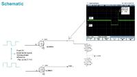
Im a newbie here would like to ask some advise on handling Inductive kick back on inductor switches that im working on.

It seems like the Mosfet(Si2308DS) (DataSheet) occasionally damage after operating a certain duration. (Drain source resistant = ~0ohm)

I found out the Absolute Max rating for the Vds = 60V, however the inductive kickback voltage seems to be higher ~70-75V.

Any Idea on which component to change in order to fix the problem?

Thanx in advance


Hi,

You need to put a small diode like a 1N4007 in parallel with each coil to prevent the high kickback voltage. Anode connects to drain, cathode to +24V.

Regards,
Chris
 

    ash3

    Points: 2
    Helpful Answer Positive Rating
Hi Chris,

Thanx for your respond. Appreciate it. adding the diode will actually pulled it the spike down to 24V.

Added after 1 hours 9 minutes:

Hi ,

I just found out that im going to have limitations on PCB re-layout.
Hence i need to work with the existing PCB

I did some browsing to replace the existing Mosfet Si2308DS

I found this with the same SOT23 package
NUD3124 ( Inductive load Driver) (Data Sheet)

Instead of pulling the spike down to 24V(as suggested by Chris), this NUD3124 Clamp the voltage >28V to 28V.

**broken link removed**

Im getting the samples soon,

In your opinion, will this solution workable?
 

Hello ash3,

ash3 said:
In your opinion, will this solution workable?
That looks alright to me, as long as your load current is less than 150 mA.

Regards,
Chris
 

Hi Cris,

Thanx..
i'll update the result here as soon i get the samples in..
 

I don't think, that another SOT-23 MOSFET will work better without connecting a free-wheeling diode at the inductor.

Generally, all recent MOSFETs are internally protected against inductive overvoltages by a zener diode. If the
transistor fails with inductive load, you should expect, that the stored energy respective losses in repeated switching
exceeds the transistor specification. As the energy absorbance capability is mostly dependant on chip size and loss power
capability on package, another SOT-23 most likely has the same problems.
 

Hi guys,

I got the samples in,

It seems to work fine, the cut-off of zener diodes clamp the spike at ~34V.
It seem to work fine for me
 

FvM said:
I don't think, that another SOT-23 MOSFET will work better without connecting a free-wheeling diode at the inductor.

Generally, all recent MOSFETs are internally protected against inductive overvoltages by a zener diode. If the
transistor fails with inductive load, you should expect, that the stored energy respective losses in repeated switching
exceeds the transistor specification. As the energy absorbance capability is mostly dependant on chip size and loss power
capability on package, another SOT-23 most likely has the same problems.

Hi FvM,

I do agree with you observation, however having a Zener Clamp will actually divert the energy created by the inductive kick back in to a different channel that avoids the sensitive part such as Drain - Source Junction.
 

You are right. Distributing the pulse energy over the total MOSFET area allows a much higher energy capability. This means, if
special designed devices as the said NUD3124 are not available, also an external zener clamp should be considered.
 

Status
Not open for further replies.

Similar threads

Part and Inventory Search

Welcome to EDABoard.com

Sponsor

Back
Top