Friendcheng
Junior Member level 1
hello everyone
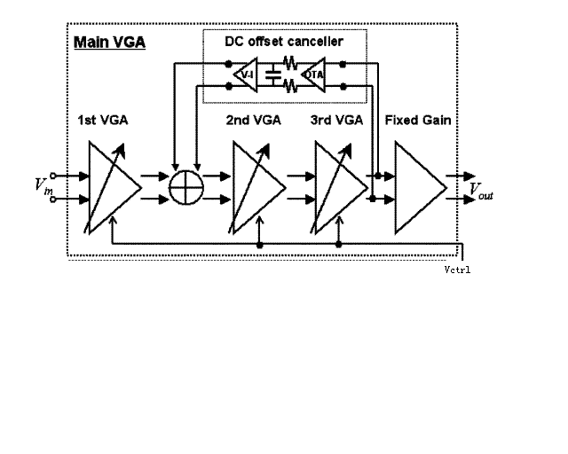
i want to do a vga in uwb system, and in many thesis it should contain a dc offset cancellation cell. In most thesis ,it contain OTA+LPF+(V-I converter) and inserted between the output of the whole VGA and the output of the first VGA cell
it's just a sketch map, and i am not clear how the V-I converter insert in the output of the 1st VGA, is the V-I converter(if an pmos) just connect the vdd(source voltage) to its source of pmos and connect the vout of the first VGA to the drain of the pmos?
can anybody told me how to connect it or recommend some thesis introduce the dc offset cancellation more clearly
thank you