Continue to Site
Follow along with the video below to see how to install our site as a web app on your home screen.
Note: This feature may not be available in some browsers.
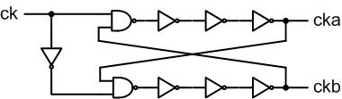
JoannesPaulus said:here is an example of a simple non-overlapping clock generator. CK is the input clock, CKA and CKB are the two non-overlapping outputs.
Added after 1 minutes:
here is an example of a simple non-overlapping clock generator. CK is the input clock, CKA and CKB are the two non-overlapping outputs.
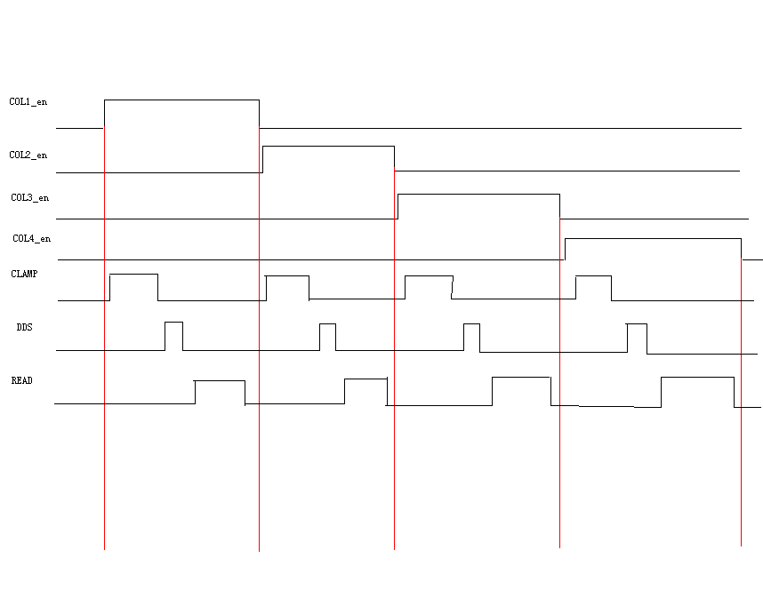
Sorry, I don't know how to post a picture.leohart said:this is a timing diagram for cmos image sensor column readout, it uses a simple sc circuits too(although there is no opamp in it)
can you post a timing diagram for the 4 non overlapped clock?
JoannesPaulus said:you can generate almost any clocking scheme once you understand the basic principle of the schematic I gave you!
kennyg said:To ricklin:
what's your reference for 4 phase nonoverlapping clock design?