Continue to Site

Welcome to EDAboard.com

Welcome to our site! EDAboard.com is an international Electronics Discussion Forum focused on EDA software, circuits, schematics, books, theory, papers, asic, pld, 8051, DSP, Network, RF, Analog Design, PCB, Service Manuals... and a whole lot more! To participate you need to register. Registration is free. Click here to register now.

16b capacitor SAR ADC test result anayse

Status
Not open for further replies.

jerryzhao

Full Member level 3
Joined
Oct 8, 2005
Messages
165
Helped
24
Reputation
48
Reaction score
4
Trophy points
1,298
Activity points
2,365
calculation of attenuation cap sar

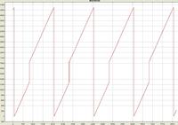
I am testing A 16 bit SAR capcacitor ADC that design by our team. There is jump voltage when the output code cross the 1/2Vr node. I can not find the root cause of this jump voltage. Anyone meet the same result? The capacitor array is control by the thermometer code. It is singal end input of ADC(AS only care the DNL in application, in order to save die size so use the singal end input).
Detail is shown in attachment figure.
 

settling time of switches in sar adc

Do you mean that there is some kind of hysteresis? Exactly how large are the jumps ?
 

what do you mean by hysteresis in adc?

the jump voltage about 8 LSB, other node 1-2 LSB. The test result very like some kind of hysteresis. But I don't think it is the comparator hysteresis. If it is the comparator hysteresis, every node will hysteresis. The ADC sample then the comparator work 16 times in SAR ADC. I don,t know why there are 2 stable state near the 1/2Vr node.
 

sar code switching dnl

It looks to me like the ADC has some "memory" of a previous compare. Some suggestions to look for:

Insufficient settling time on the DAC. This would likely worst on the MSB transition, as you are seeing. If the DAC has not settled to 16bits (>11 time constant settling) before the compare, there will be errors, which could be similar to what you are seeing. The capacitance being switched is larger for the MSB transition, which could cause the largest error to occur at that point.

Incomplete reset of the DAC between measurments.

Feedback from the comparator to the inputs when the compare is performed.
 

    jerryzhao

    Points: 2
    Helpful Answer Positive Rating
sar adc series cap

I think some "memory" is root cause. I am looking for some way to prove it.
 

Every comparator has some sensitivity i.e it does not see change below some limit.
This limit has to be much below LSB (~LSB/10 ie.e ~uV)in order not to disturb dnl and inl characteristics. It does not cact as a constant offset-it depends on signal amplitude...When signal amplitude between threshold and comparator voltage is high you will not see such effect, but if comparator voltage is in the area of comparator threshold it will make error. For the most of codes you will not notice this effect. Can you simulate comparator input around this point

Is this differential or single ended varuiante? Which type of comparator have you used? Does it have some type of autozero?Do you use some kind of error correction?
 

One way to test for insufficient settling time in the DAC would be to run the ADC with a slower clock. If the problem decreases or is eliminated, then a settling time issue is most likely the cause.
 

There are 3 stage pre-amp the last stage is a latch for comparator. The comp is differential input, one end connect cap array output, other end connect the VCM.
There are restet swith in pre-amp, there are output voltage limit diodes in pre-amp. the latch can autozero. But without the offset cancel in comparator as our system is not care the offset.

I test the ADC in low speed, when the SPS less than 10Ksps the jump voltage do not reduce as the sps reduce. 10K-30K SPS the jump voltage increase with the sps speed increase.

Added after 5 minutes:

I simulate the voltage around the VCM, the comparator result is right. We do noise simulation simulation also. so we can test the DNL is 1~2 LSB in most point. only the jump vlotage in when input cross the 1/2 VREF.
 

jerryzhao said:
There are 3 stage pre-amp the last stage is a latch for comparator. The comp is differential input, one end connect cap array output, other end connect the VCM.
There are restet swith in pre-amp, there are output voltage limit diodes in pre-amp. the latch can autozero. But without the offset cancel in comparator as our system is not care the offset.

I test the ADC in low speed, when the SPS less than 10Ksps the jump voltage do not reduce as the sps reduce. 10K-30K SPS the jump voltage increase with the sps speed increase.

Added after 5 minutes:

I simulate the voltage around the VCM, the comparator result is right. We do noise simulation simulation also. so we can test the DNL is 1~2 LSB in most point. only the jump vlotage in when input cross the 1/2 VREF.


With segmented coding you can not have problem at Vref/2. Also capacitance mismatch does not depends on sampling ratio.
Problem comes from some dynamic element - probably comparator. Note that at Vref/2, equivalent capacitance between Vref and gnd is highest. Is Vref good enough?
You have to add some non ideality into the schematic.
For example 2-10fF parasitic capacitance at the one side of the latch, can produce non-constant offset. Try to slightly add mismatch into a comparator preamolifier, for example increase slightly W/L ratio at the one side of the preamplifier.
How much is the total gain of the 3 stage preamplifier?
 

In order to low 1/f noise, the input thransistor size is very large that is 4000/0.5, the loading transis is doide connect size is 120/4. in order to increase the gain of preamp, the designer add a positive feedback transistor parallel with the diode connect transistor size is 96/4.
First I think maybe there is hysteresis in comparator as mismatch by those positive feedback transistor, then I add mismatch in thoes load transistor but I don,t find the hysteresis.
In SAR ADC the system sample then comparator run 16 times. the comparator reset when system sample, so the hysteresis will affect the resolution, not a jump voltage when input cross the 1/2VREF(or code cross the 10000...00).

Added after 3 minutes:

The reference come from external low noise LDO. the gain of 3 stage is more than 100 dB, the open loop -3 dB bandwith larger than 3.5M(worst case).
The normal sample rate 60K sps.

Added after 22 minutes:

The cap array first time output is (VCM-Vin)+1/2Vr. When the vin little large than 1/2Vr, the cap array will become 3/4 vr then SA to near 1/2Vr. When the Vin little less than 1/2Vr, the cap array will become 1/4 vr then SA to near 1/2Vr. this jump voltage effect like a "memory" in system. but only the cap array is floating node when comp run. Did the charge injection from VCM swith? (the system sample the cap array output node connect VCM, and the vcm switch turn off first, in order reject the input switch charge injection). But I think this charge injection should be only a offset. Does is it relate to input amp? Or the voltage can change the cap value? But I use the MIM cap.
I am try my best to find the root cause. Thanks your help. any comments please let me know. Thanks.
 

Dou you use fully differential or single ended capacitor array?
Are all capacitors parallel or you use 2-stage architecture with serial cappacitance attenuation?
Have you tried mismatch with parasitic capacitance 5fF at the latch, or preamplifier output... that can make memory effect.
You can see non-linearity coefficient in your process specification. cmim should be better than cpoly.
But if you use segmented architecture you switch only C0, which should not produce such error, specially at Vref/2. Try to calculate.

Can you plot voltage at the input of the comparator?
 

Hi,
Can you give one more data - how the VCM is generated? From the total discussion, it seems like the problem is not from comparator and DAC settling as well. Again, the error is near VCM. It looks like a single ended implementtaion of the CAP array and VCM is generated independent of the CAP array.

How the VCm is generated? Does it having any dependency on MSB/MSB-1 switching? Anay coupling between C-DAC output and the VCM node which may be more at mid-code?

I primarily suspect the above as the pattern from 00--00 to 11--11 and the reverse missed almost the same codes. It looks like, the CDAC and Comparator combination can-not see (identify) the these codes irrespective of the situation. Looks like VCM is some how having a dependency of input signal swing and MSB/MSB-1 switching. This may hide the codes to appear from the ADC output.

Anyway, its interesting. Any progress you should write here.

Could you do one more thing, test the ADC near the VCM zone with reduced Vrefs, such as to zoom in to the centre to diagnose. And the steps should consists of low clock speed (may be 1KSPS) and both very slow ramp to input and max allowable rap to input.

sankudey
 

It sounds like settling time is not the issue.

Next thing that comes to mind: Is the preamplifier always in the same state at the sampling time? It could be that the preamplifier goes from being saturated in one direction to saturated in the other direction when the sampling switches are closed. I am not sure how to verify this one, other than if you can show the problem in simulation.
 

and why do you use thermometer code decoder?how do you control the thermometer code switching capapcitor? is it same switch sequency for the different ADC input direction?
 

I have run the simulation add the parasitic cap at latch input, but I didn't find the memory effect.

The VCM come from resistor devider following by OP buffer. the VCM external to PIN, and there are 10uF&1uF cap in VCM PIN on PCB. I don,t think it depend on VCM, as we external a VCM voltage, the jump still at 1/2VR(code 011..11 to 1000...).

The preamp still run with clock when ADC sampling.I don't think that is a good design. So the preamplifier is not always at the same state when sampling time. But the simualtion can not find that affect.

I do full ADC test, I find there are the jump voltage at 1/4 3/4VR 1/8 3/8 5/8 7/8VR.
The jump voltage is 8LSB at 1/2VR(ADC output code 0111..to 100.00) The jump voltge is 6LSB ar 1/4 3/4 VR(ADC output code 0011111.. to 010000..0) the jump voltage is 4LSB 1/8 3/8 5/8 7/8 VR.

Added after 4 minutes:

There 2 section in cap array in ADC, 7bit + 9bit. signal end input. the coupling cap between two section is unit cap, so the LSB section is 127 unit cap.
XYdecode control the thermometer code. the control circuit design by digital designer.
 

jerryzhao said:
There 2 section in cap array in ADC, 7bit + 9bit. signal end input. the coupling cap between two section is unit cap, so the LSB section is 127 unit cap.
XYdecode control the thermometer code. the control circuit design by digital designer.

This configuration is sensitive to parasitic capacitance to the ground, and to a mismatch of serial cappacitance. Try to open a model and to see is this capacitance modeled.
Put some parasitic capacitance at one side of the coupling capacitor, or to add mismatch to coupling capacitor. It seems that there could be a problem, if you also have step at 1/4, 3/4 Vref... But I dont know why is there hysteresis.
 

I have calculate the mismatch, I do some simulation, all the mismatch or parasitic cap only contribute a offset, not the hysteresis. I am looking for.........
 

jerryzhao said:
I have calculate the mismatch, I do some simulation, all the mismatch or parasitic cap only contribute a offset, not the hysteresis. I am looking for.........
Note that offset does not appear into a total characteristic as a constant offset, because you have to connect two DACs. It degrades dnl and can produce such jumps, which are code dependant.
If you use serial capacitance it has at the bottom side parasitic that can go up to 30%
This does not have anything with hysteresis? Can it be measurement error?
 

I measurement many time, always see the hysteresis, I know the parasitic cap of couping cap, will lead a jump voltage, in my old design(12bit) ADC I see this effect. but that jump voltage is at the LSB section to MSB section node, not at the 1/2vr, 1/4vr etc. that jump without hysteresis.
 

Dear zhao,I had also meet this problem in my early design.At last,we find the root cause was because layout engineer did not put the DAC size value in LVS check.Do you want check it again.Other question, do you have self calibrating circuit in your 16bit sar adc design?I think design a 16bit SAR ADC is not a easy task.
Added my test result.
53_1214818293_thumb.jpg
 

Status
Not open for further replies.

Part and Inventory Search

Welcome to EDABoard.com

Sponsor

Back
Top