vikash23
Full Member level 2
Hi,
I am trying to implement a sine wave generator for 5KHz, 7V pk-pk using 555 timer.
Using LTspice and online resources I did the following circuit.
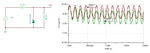
I can able to achieve the 5KHz, 7V pk-pk after the capacitor C4. My aim is to do a zero offset of the signal and I have implemented the NE555 U3 circuit.
But I couldn't achieve it.
Do I need to use an op-amp and a negative voltage to achieve a zero offset of my output signal?
I have attached the image of my LT spice.. Green traces are from C4 out. Blue traces are from NE555 U3 out.

I am trying to implement a sine wave generator for 5KHz, 7V pk-pk using 555 timer.
Using LTspice and online resources I did the following circuit.
I can able to achieve the 5KHz, 7V pk-pk after the capacitor C4. My aim is to do a zero offset of the signal and I have implemented the NE555 U3 circuit.
But I couldn't achieve it.
Do I need to use an op-amp and a negative voltage to achieve a zero offset of my output signal?
I have attached the image of my LT spice.. Green traces are from C4 out. Blue traces are from NE555 U3 out.