Continue to Site

Welcome to EDAboard.com

Welcome to our site! EDAboard.com is an international Electronics Discussion Forum focused on EDA software, circuits, schematics, books, theory, papers, asic, pld, 8051, DSP, Network, RF, Analog Design, PCB, Service Manuals... and a whole lot more! To participate you need to register. Registration is free. Click here to register now.

[SOLVED] What is OD (oxide diffusion) and why is it considered as part of the WPE

Status
Not open for further replies.

Arokia

Newbie level 6
Joined
Oct 23, 2017
Messages
12
Helped
0
Reputation
0
Reaction score
0
Trophy points
1
Location
RR Nagar, Bangalore
Activity points
124
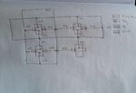
image of od example.jpg


For example in the above image, we can understand that, the Nwell will have a higher doping concentration at its edges. But when we consider the OD layer, the <AND> operation of the P-implant and the OD layer is what creates the diffusion (ie the sorce or drain). So like the N-well, the edge of the OD will be the edge of the source or drain right? So if the OD layer does not have its own edge which is spaced apart from the transistors (npn or pnp), then why is it considered in the Well proximity effects in 28nm TSMC technology. Can someone please shed some light on this question.
 

Not being familiar with this node or process flow,
can't say whether OD is the same as active area
/ thin ox (not indicated).

AA is often a "hard mask" with Nimp/Pimp only rough
constraints on where S/D implants are shot (so N+
= AA*Nimp).

Proximity effect, "to what?", is a question. Maybe
STI is !OD or maybe it isn't. Again have to go to the
process flow and realistic cross-section views, not
this LGRP-looking sketch.
 

Thick Oxide (OD2) Layout Rules

Define thick oxide area of 1.8v or 2.5v I/O transistors
The OD_25 Layer (CAD layer: 18) is used for 2.5V gate oxide area.
The OD_18 Layer (CAD layer: 16) is used for 1.8V gate oxide area.
OD2 refers to any thick oxide device, for exmple OD2=OD_18, OD_25.

Based on the above information, the OD layer in the diagram is actually the OD2 layer which is a thick oxide layer (dielectric) to change the gate voltage.

Now the question is how transistors at the edges of this OD2 layer have different properties when compared to transistors at the center of the OD2 layer (or non edge of the OD2 layer). It makes sense for the N-well because the doping concentration at the edges of the N-well is higher compared to the normal doping concentration at the non edges of the n-well. But how does it make sense for the OD2 Layer (Thick Oxide Layer (Dielectric)), is it that at the edges of the OD2 layer, there is mechanical stress due to etching (or over etching) and hence, the properties of the transistors are different. Please provide your valuable thoughts.
 

Your drawing is not making sense to me partly because everything looks black except the red nimp/pimp. Which doesn't make sense. Looks like red should be poly which cuts across active to form the transistor. The top two transistors are thick ox , the left two are in nwell so those are pmos. But you have no p or n implants.

Now to your question. There shouldn't be any transistor property differences due to a thick ox layer. There will be differences with transistors that share a common active area due to STI stress.
 

Given this explanation, OD2 is a companion to AA and in
my experience, simply prevents a second AA oxide etch
(the "thick" oxide being a combination of two gate ox grow
steps, thin being only the second of the two).

Now transistors with thicker gate ox have less channel
authority over edge oxide quality / charging effects, so
are likely more sensitive to STI or LOCOS quality and
proximity. At least they must be presumed different until
qualified.

Where you get these ideas about "shouldn't", I dunno.
But I've done many transistor curve pulls (for reasons
/ environments I won't discuss here) that sure did expose
gross differences in edge behaviors between co-processed
"thin" and "thick" devices.

Not to say that the rules couldn't be entirely made up.
But there are real differences in construction so real
electrical differences (perhaps subtle, perhaps not) are
to be expected.
 

1. OD = active = diffusion = moat; STI = NOT OD

2. WPE = Well Proximity Effect - dependence of transistor Vt on its location with respect to well edge (at the well edge, doping density is different than in the middle of the well, due ion scattering at mask edge during ion implanation.

3. LOD - Length of Diffusion effect - mechanical stress in MOSFET channel depends of the distance from the channel to the edge of diffusion region, that affects device characteristics (mostly mobility).

LOD is not a part of WPE, but a part of LDE - Layout Dependent Effects, that are important in (relatively) advanced technologies.
 

Arokia - this diagram does not make sense to me, it does not look right, if these are transistors and not some unusual structures.
If blue is poly, then red should be OD.
Each poly should be within NIMP or PIMP (or withi NIMP OR PIMP).
 

Looks like i've finally understood that OD2 would be an implant layer, which would change the doping concentration underneath a transistor (this is mainly done to vary the Vth (threshold voltage) value as per the circuit designers requirement. For example if the Vt value of a normal transistor was 1V, transistors placed inside this OD2 layer, would have a different doping concentration in the P-substrate incase of NMOS and NWELL incase on PMOS, for instance 1.8V.

This was clearly indicated, in the circuit diagram, when they used the subtype "pch_hvt" instead of "pch"

Now moving on to the actually question, "why should we be following the WPE rules when using the OD2 layer", well the answer to that would be, since we are using OD2 layer to change the doping concentration, there are chances of having higher concentration towards the edges, due to refraction during the implantation process. So placing transistors at the edges of the OD2 layer would disrupt any sort of matching that is done for analog layouts, as they would have a Vt value that is different from 1.8V.
 

It's very unusual to have the same implant for Vt adjustment of both nMOS and pMOS FETs.

Also, the name OD2 being used for implant is very unusual.

The design rule manual for the technology should explain the meaning of all layers, there should be no guessing.
 

What is OD (oxide diffusion)

Several decades ago I've learnt OD means (oxide) Opening for Diffusion, i.e. the mask for (thick) oxide etching to allow for subsequent diffusion (nowadays: implant), cf. this snippet:
OD__Opening_for_Diffusion.png
 

@Max: Thank you! But sometime after STI etch, filling & CMP, the active area (AA or OD) FOX has to be removed for subsequent implant, isn't it?

BTW: the OD oxide diffusion naming (s. thread title) I perceive as rather deceptive.
 

erikl -

"oxide diffusion" is an oxymoron, but it is a very widespread oxymoron, so I guess we have to live with that.

I think FOX stands for Field Oxide - wichi is oxide layer fillign the STI (outside active/diffusion).

I think layer OD defines the mask used for STI etch, so what is not etched is OD = active = diffusion = moat = ...
It seems all these terms have their roots in older technologies where many things were very different from present day technologies.
 

Hi Maxim,
"oxide diffusion" is an oxymoron ...
Yeah, that's the right designation! What a nice similarity of ox.. terms :-D

I think FOX stands for Field Oxide - wichi is oxide layer fillign the STI (outside active/diffusion).
Field Oxide in general. Also the original (very first) full-wafer oxide. Sometimes called thick oxide, too.

... OD = active = diffusion = moat = ...
Right!
 

Status
Not open for further replies.

Part and Inventory Search

Welcome to EDABoard.com

Sponsor

Back
Top