Continue to Site

Welcome to EDAboard.com

Welcome to our site! EDAboard.com is an international Electronics Discussion Forum focused on EDA software, circuits, schematics, books, theory, papers, asic, pld, 8051, DSP, Network, RF, Analog Design, PCB, Service Manuals... and a whole lot more! To participate you need to register. Registration is free. Click here to register now.

Simulation of hierarchy design does not work !

Status
Not open for further replies.

msdarvishi

Full Member level 4
Joined
Jul 30, 2013
Messages
230
Helped
1
Reputation
2
Reaction score
1
Trophy points
18
Activity points
2,349
Dear all,

I am using ISE 14.7 targeting a Virtex-5 FPGA. I wrote a VHDL code for the attached figure containing a clk50MHz module, an LFSR and a pulse counter.

The clk50MHz has an input clock of 100MHz and provides a 50MHz clock at its output to feed the LFSR.
The LFSR is used to generate random pattern as an input pulse for pulse counter module.
The pulse counter measures the period of its input signal (here is the 7th bit of count output in LFSR)

While I simulated each module individually in the hierarchy design, their corresponding testbench and the results are very nice and they work !
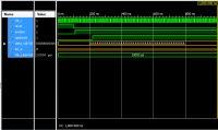
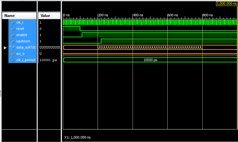
They problem is when I try to simulate the whole Top module that contains all three sub modules (clk50MHz, LFSR, and pulse counter). As you see in the attached timing diagram, the data_o output goes to UUUUUUUUUUUU state while the pulse counter works very nice. I tried to see the action of submodules in simulation of Top file and I see the LFSR receives the 50MHz clock as its input clock but it does not start counting !!!!

It is noticable that I have assigned the DATA_O signal to '0' state at the beginning of testbench but it does not work !!

I also attached the design files. Can anybody help me to solve this problem? My case is urgent and I do not know how to solve it ?!! Kind replies and helps are mostly appreciated.

Regards,

fig1.png

View attachment sources.rar
 

Odds are, it is not that "simulation does not work". It probably
is returning plain facts, that something is unknown.

I observe that your pulse counter has no reset pin. So how
is it getting an initial state? Perhaps the question is, why
did it (if it indeed did) work standalone?
 

In a standard case when the pulse_counter is fed with the reset signal, its output should be 0/0s. That how the logic should be designed. If you don't have a reset input modify your design to have one. So apart from what is told in #2, i would also suggest you to observe all internal signals. Specially the signals going in/out from one to the other.

Any signal showing values U/Z should be a pint of concern.

Also I see that your LFSR and pulse_counter are fed with 50MHz and 100MHz clocks. Two different clock domains. So you should be careful here too while constraining your design.


Dear @dpaul,

Thanks for your reply and explanation. In the first post, I forgot to add the Top.vhd file in the attachement. Here you find a full package of design files.

Concerning the RESET pin for pulse counter, you're right, I will modify the design to have it there.

Concernining the use of two clock signals, it is obvious that the pulse counter must be clocked at least twice faster than the circuit uncer test (here LFSR) in order to be able to measure the peiod of input pulse. Regarding the constaints, there was no harmful issue on that and I will pay attention to it as well.

Concerning verification of internal signal, that is what I am doing, I look at signals of each sub-module (clk50MHz, LFSR, and pulse counter) and as you can see from the new attached source files, the LFSR receives the 50MHz clock signal but it does not start counting to generate the output pattern !! It seems weird ! Do you have any idea, please?

Thanks and Regards,
 

Attachments

  • sources_full.rar
    3.6 KB · Views: 70

I have assigned the DATA_O signal to '0'
How? It must be reset in the counter module, or hierarchically forced.

I fear, the nice schematic design representation is almost useless without seeing the actual module definition and test bench.

It's probably not a problem of hierarchical simulation, just missing signal initialization.

- - - Updated - - -

Just noticed you posted the sources in the meantime.


Dear @FvM,

Thanks for your reply. I managed the design to include reset pin in pulse counter as well. Here in the attachment you see the full list of files with their test benches. Do you have any idea about them?

Thanks and Regards,
 

Attachments

  • sources_full_tb.rar
    9.6 KB · Views: 66

I don't use Xilinx tools. A reasonable simulator like will tell you where the design problem is, Modelsim informs about 'X' in arithmetic operation in module_LFSR. If you look into it, you see that the synchronous reset fails, because the clock is inactive during reset pulse. Suggestion: Use asynchronous reset throughout the design.
 

Just as I suspected, your LFSR code is not coming out of reset properly, because you've got a logic generated clock (a poor design decision in an FPGA) driving the component.

You used the reset to initialize the clk_o generation, so clk_o does not start toggling until after the reset has already gone away.
Because you used a synchronous reset in your LFSR code, it never sees the reset so stays U.
Code:
        if (rising_edge(clk)) then
            if (reset = '1') then
Make the reset in the LFSR an asynchronous reset and get rid of all the extra signals in the process sensitivity list. There should only be clk and reset in there.

Also get in the habit of using a real text editor not the crappy one in ISE, it doesn't know how to manage the difference between CR-LF and LF so all the files end up with a mix and when read in by VIM you get the following results:
Capture.PNG

Notice the ^M stuff that is VIM seeing the LF as the default (unix style) and displaying the CR character separately.
Note the hideous red stuff is your silly mix of tabs in code that also uses spaces. Use spaces only as you'll notice my tabs don't match your tabs, and probably don't match 3/4 of the people out there. Stick with spaces and your code will always look properly formatted. Of course that doesn't stop another newbie from editing your file with their screwed up text editor ;-)
 

Status
Not open for further replies.

Part and Inventory Search

Welcome to EDABoard.com

Sponsor

Back
Top