Continue to Site

Welcome to EDAboard.com

Welcome to our site! EDAboard.com is an international Electronics Discussion Forum focused on EDA software, circuits, schematics, books, theory, papers, asic, pld, 8051, DSP, Network, RF, Analog Design, PCB, Service Manuals... and a whole lot more! To participate you need to register. Registration is free. Click here to register now.

Opening PCB file with Pads 2005 sp2

Status
Not open for further replies.

yassinevic

Newbie level 3
Joined
Nov 24, 2015
Messages
3
Helped
0
Reputation
0
Reaction score
0
Trophy points
1
Activity points
23
HI

can anyone helps me to get a screen-shots of the layout in this pcb file?
it needs PADS 2005 SP2 to be opened, and i can't find a link to download it anywhere.
View attachment H85-03LFC-MAIN.zip

Tnx in adavnce
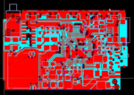
 

Opens just fine in Pads 9.5, what do you need to see?

It is a 4 layer board, with some interestingly poor EMC design from the look of it.

Capture.PNG
 

Yes, it's very poor design as you mentioned.
I was hooping to get the pinout layout of the EAT5767 used as FM module "the empty bottom left area".

It's the PCB of a chines mp3 device i post in this thread.

https://www.edaboard.com/threads/347442/
 

Status
Not open for further replies.

Part and Inventory Search

Welcome to EDABoard.com

Sponsor

Back
Top