Continue to Site

Welcome to EDAboard.com

Welcome to our site! EDAboard.com is an international Electronics Discussion Forum focused on EDA software, circuits, schematics, books, theory, papers, asic, pld, 8051, DSP, Network, RF, Analog Design, PCB, Service Manuals... and a whole lot more! To participate you need to register. Registration is free. Click here to register now.

nakagome charge pump doubt

Status
Not open for further replies.

learning_curve

Member level 1
Joined
Sep 10, 2010
Messages
38
Helped
3
Reputation
6
Reaction score
3
Trophy points
1,288
Activity points
1,518
Hello,

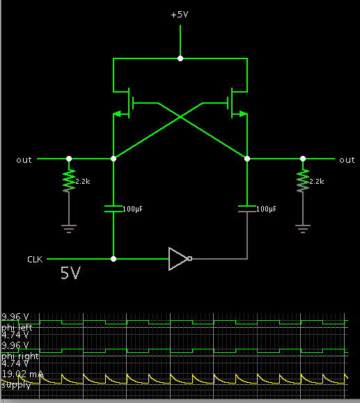
I was looking at the nakagome charge pump circuit...please refer attached pic nakagome.png


I am unable to understand how the final value of phi+VDD and phibar+VDD gets established..
need some help tracing the voltages ..
 

I like to explore unfamiliar circuits using the animated simulator at www.falstad.com.

Charge pumps are always interesting. So I tried your Nakagome.

Here is a screenshot with scope traces:


It needed loads attached, to maintain charge pump action on the capacitors.

The supply, clock and inverter are all 5V.

As you can see, the outputs alternate between 5 and 10V.

This software has the capability of exporting an entire layout as a weblink. In case you would like to run the same simulation...

Just click the link below to open the website, load my schematic automatically, and run it on your computer.

Click Allow when it asks for permission to open the Java applet.

https://tinyurl.com/9ypgc9t
 
thank you Bradtherad,

It makes sense the outputs switch between 5 and 10 V depending on if CLK is 0V or 5V. I will simulate it.
I was trying to see what happens before the outputs reach the final values of 5 and 10V.
As in how the circuit starts and builds up to those final voltages...
 

Status
Not open for further replies.

Similar threads

Part and Inventory Search

Welcome to EDABoard.com

Sponsor

Back
Top