Continue to Site

Welcome to EDAboard.com

Welcome to our site! EDAboard.com is an international Electronics Discussion Forum focused on EDA software, circuits, schematics, books, theory, papers, asic, pld, 8051, DSP, Network, RF, Analog Design, PCB, Service Manuals... and a whole lot more! To participate you need to register. Registration is free. Click here to register now.

how to reduce parasitic resistance on the layout

Status
Not open for further replies.

allennlowaton

Full Member level 5
Joined
Oct 5, 2009
Messages
247
Helped
3
Reputation
6
Reaction score
3
Trophy points
1,298
Location
Taiwan
Activity points
3,066
Hello EDA fellows,

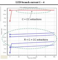
The graph below shows the post simulation using the R+C+CC and C+CC extractions.
The problem can be traceable to the parasitic resistance.
The expected result is the same as that of the C+CC.
My concern now is how to reduce the parasitic resistance in the layout.


No. The parasitic resistance being obtained from the layout.
 

I have no idea on specifics of LED and associated Layout.
In general :
1. Widen the wires if possible [not violating DRC of course].
2. In case there are multiple metal layers - between layers in case you have VIA - increase the number of Via-counts in parallel, that will reduce parasitic resistance.
 
Status
Not open for further replies.

Part and Inventory Search

Welcome to EDABoard.com

Sponsor

Back
Top