manalog
Newbie level 4
Hello all,
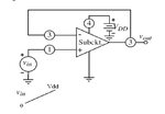
Today I have simulated an Two-stage opamp to find out its ICMR.
To find out ICMR i gave dc input @ VIN+, & VIN- is connected to VOUT. And plotted VOUT after DC simulation.
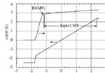
As nmos differential pair is used at input, i was expecting the VOUT to be linear from V1 to VDD ( where V1 > GND ). But surprisingly, VOUT vs VIN+ plot shown the linear result. means VOUT is following VIN+ linearly (like rail-to-rail opamps)!!!!!
so when i checked manually, i found some transistors are not in saturation region!!!!
some books say "ICMR is the range over which all transistors will remain in saturation".
and Allen's book says "ICMR is the range over which amplifier amplifies the diff signal with same gain".
as it obvious that gain will reduce if all transistors are not in saturation.
So does it mean to find out the ICMR (DC characteristic of opamp) i need to do AC simulation?
And if i do the DC simulation i need to check all transistors operating region manually?
Or is there any other method to find out ICMR?
PLZ HELP...
Today I have simulated an Two-stage opamp to find out its ICMR.
To find out ICMR i gave dc input @ VIN+, & VIN- is connected to VOUT. And plotted VOUT after DC simulation.
As nmos differential pair is used at input, i was expecting the VOUT to be linear from V1 to VDD ( where V1 > GND ). But surprisingly, VOUT vs VIN+ plot shown the linear result. means VOUT is following VIN+ linearly (like rail-to-rail opamps)!!!!!
so when i checked manually, i found some transistors are not in saturation region!!!!
some books say "ICMR is the range over which all transistors will remain in saturation".
and Allen's book says "ICMR is the range over which amplifier amplifies the diff signal with same gain".
as it obvious that gain will reduce if all transistors are not in saturation.
So does it mean to find out the ICMR (DC characteristic of opamp) i need to do AC simulation?
And if i do the DC simulation i need to check all transistors operating region manually?
Or is there any other method to find out ICMR?
PLZ HELP...