sjamil02
Member level 4
- Joined
- Nov 8, 2009
- Messages
- 72
- Helped
- 9
- Reputation
- 18
- Reaction score
- 5
- Trophy points
- 1,288
- Location
- United Kingdom
- Activity points
- 1,961
Hi All,
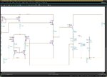
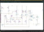
I attach the schematic (including dc node voltages) for LDO with two-stage OTA and PMOS power device. In order to get dropout voltage of 35mV, I used the following equation to size up the PMOS. W/L=(2Id)/(kp*vdssat2) and vdssat=35mV. I end up with a very huge PMOS, W/L=469153. The regulation voltage Vreg is set based on the following, Vreg=(1+R2/R1)Vref where Vref=0.9V, R2=3.6k and R1=50k. When I put the circuit together and run dc and ac simulation, from ac simulation the gain is below unity. The nmos (x11) of the output stage of an OTA is in triode (vds=59mV). How do I fix this problem? How to size the PMOS to minimize the size while still be able to achieve vdropout=35mV? It seems from my calculation the size is too big!
Please help.
Thks in advance
sj
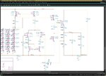
") ). The problem now is since the PMOS has to be in triode, its gate voltage is very close to gnd i.e. Vgate=35mV and VSG=1V. (see schematic). The output of the feedback amplifier swing close to gnd and nmos (x11) in triode and hence the amplifier gain drop below unity. If I understand it correctly, the feedback amplifier's output range need to be able to swing close to gnd while still operate in saturation? What is suitable topology to remedy this problem? Class AB output stage? Or is there any simple solution to my problem described here?
). The problem now is since the PMOS has to be in triode, its gate voltage is very close to gnd i.e. Vgate=35mV and VSG=1V. (see schematic). The output of the feedback amplifier swing close to gnd and nmos (x11) in triode and hence the amplifier gain drop below unity. If I understand it correctly, the feedback amplifier's output range need to be able to swing close to gnd while still operate in saturation? What is suitable topology to remedy this problem? Class AB output stage? Or is there any simple solution to my problem described here?