Continue to Site

Welcome to EDAboard.com

Welcome to our site! EDAboard.com is an international Electronics Discussion Forum focused on EDA software, circuits, schematics, books, theory, papers, asic, pld, 8051, DSP, Network, RF, Analog Design, PCB, Service Manuals... and a whole lot more! To participate you need to register. Registration is free. Click here to register now.

Queries on gm/id methodology

Status
Not open for further replies.

Ravinder487

Full Member level 3
Joined
Jul 9, 2010
Messages
169
Helped
0
Reputation
0
Reaction score
0
Trophy points
1,296
Location
Bangalore, India
Activity points
2,469
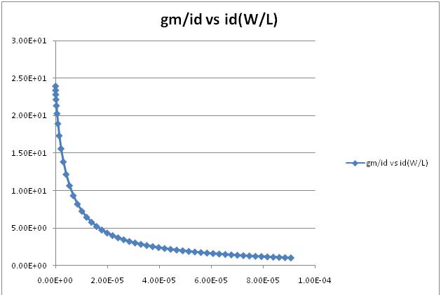
Can we use SPECTRE for plotting gm/id graph?My gm/id plot isn't looking similar to that shown in textbooks.Max value of gm/id in my graph is around 400 but literature says it should be maximum of 36.
After getting W/L values from gm/id plot how should we bias the circuit so that all transistors are in saturation.
If a transistor is in weak inversion then it is saturation or triode?What will SPECTRE show.
 

Hi Ravinder487,

Sure you can get this from spectre.Follow this chain : ADE L's top menu --> Tools --> Results Browser , search for gmoverid and plot it.Maybe it is needed to create a file that saves the operating point first,so check my post at 23-08-10 18:46 here https://www.edaboard.com/threads/186018/ for the respective how to.

Take a look at this book for more info about gmoverid analysis :

The gm/ID Methodology, a sizing tool for low-voltage analog CMOS Circuits: The semi-empirical and compact model approaches (Analog Circuits and Signal Processing) by Paul Jespers

Don't confuse the inversion level (weak,moderate,strong) of a transistor with the region of operation (triode,saturation).I would propose that you read some transistors' basics first before going deeper in analog design.

Regards,
Jimito13
 
  • Like
Reactions: johnGu

    johnGu

    Points: 2
    Helpful Answer Positive Rating
Hi jimito,thaks for ur reply.But as per my perception operating transistor well below threshold is weak inversion region and far away from threshold is strong inversion and the intermediate region is moderate inversion.I don't know whether there are any restrictions on Vds.
I think its better if you give some brief idea on these concepts.

---------- Post added at 12:09 ---------- Previous post was at 11:56 ----------

Error found by spectre during circuit read-in.
"/home/ravi/Desktop/sigtype.scs" 0: Syntax error in save statement.This is error I'm getting when I included sigtype.scs file in modelfiles library
 

Yes,your perception about inversion level is correct but don't confuse these definitions with the region of operation for a transistor (triode,saturation).For an nmos device when Vds<Vdsat you are in triode and when Vds>Vdsat you work in saturation.That's all!

Apparently you have some syntax error...Maybe a snapshot of your file and the error's would be better for a helpful feedback ;-)
 
Last edited:

I am not totally sure but i think that this is a bug of older versions of MMSIM...What version do you use?Try to upgrade to MMSIM 7 to solve this.

Another approach is to save the op point just for the device you care (e.g. : save T1:eek:ppoint).Does this work?

Or you can try this syntax : save *:eek:ppoint
 
Try to change the initial syntax to the other two i suggested above.If these don't work then the only solution is to upgrade your MMSIM (ask your CAD Administrator,he should know the procedure for this it is easy).
 
you are using spectre from IC stream, use spectre from MMSIM stream. I think after MMSIM62 wildcards (*) are supported.
 
Hi jimito,
I have one basic question over gm/id plots.Some materilas from net say that I need to connect transistor as diode connected and i need to sweep the gate(which is also drain) voltage and plot gmoverid and some other say that I need to fix drain voltage and sweep gate voltage.
which of these two configurations is correct and why?
 

Hi Ravinder487,

The answer depends on versus what quantity you want to plot the gm/ID.Usually we want to plot gm/ID versus ID/S,where S=W/L (Shape Factor) in order to achieve an optimum sizing for the transistors from the graph we previously extracted.Maybe what you read concerns a specific aim...so if you post the exact links here we can clarify your question better.

Regards,
Jimito13
 

I'm attaching 2 files which I've referred.gm/id curves are specific to a given technology and are well defined ,hence there will be only one best configuration that minimizes non-linear effects.
 

Attachments

  • gm-id-examples_1619.pdf
    1.6 MB · Views: 249
  • gmid_ruida_5888.pdf
    208.5 KB · Views: 248

... which of these two configurations is correct and why?
Correct are both methods, I think. The diode connected configuration, however, doesn't well reflect the MOSFET's operation region which normally is used for amplification: saturation region. Working with Vds=Vgs means operating on the intercept point between triode & saturation region (or not very far beyond, if in moderate/weak inversion), i.e in a region below optimum output impedance (ro, or "Early-Voltage/Id").

This is not what you would want for a gain stage. So I think the gm/Id measurement with a fixed Vds - as in the Ruida Yun paper - comes closer to a real application. The diode connected measurement - in contrast - would show the lower limit of attainable gm/Id vs. Vov .
 
Hi erikl thanks for your reply.I need your suggestions in designing simple two stage opamp.I have tried gm/id methodology to find W/L of every transistor but I don't know how to fix Vin,cm of the differential pair.
And I don't think that this gm/id will work for designing OTA in 90nm technology
 

@erikl:I'm attaching my gm/id vs id/(W/L) plot.If I choose a value of 10 for gm/id then my corresponding value of id/(W/L) is 72uA.With bias current as 45uA(considering slew-rate requirements and power dissipation) my W/L should be less than 1 and with this value of W/L i will never achieve a gain of 100.
And in the file you have attached I find only gmid plots but not any design examples.I need step by step method of designing OTA using gm/id methodology .Please help me in these matters.Thanks in advance.
 

You must specify your circuit so that we can give you some guidelines...Speaking generally about design methodologies will never lead you to a result!

Anyway,some references can be found in the attachments i uploaded for you,but i repeat : you must provide more info about your design and the specs you are aiming.
 

Attachments

  • 05533393.pdf
    181.6 KB · Views: 481
  • v45-6.pdf
    454.7 KB · Views: 253

I want to design simple differential amplifier with active load as first stage and CS amplifier as second stage.
I want to know how to fix common mode voltage of differential pair after getting W/L ratios from gm/id plots.Can you please read out W/L ratios from my gm/id plot attached above for a bias current of 45uA
 

Do the gm/id plots vary with channel length?Because I'm getting different gm/id plots for 100n and 300n.Here is the plot I'm attaching gmid plot for L=300n,earlier I've attached gmid plot for 100n
 

Status
Not open for further replies.

Part and Inventory Search

Welcome to EDABoard.com

Sponsor

Back
Top