Continue to Site

Welcome to EDAboard.com

Welcome to our site! EDAboard.com is an international Electronics Discussion Forum focused on EDA software, circuits, schematics, books, theory, papers, asic, pld, 8051, DSP, Network, RF, Analog Design, PCB, Service Manuals... and a whole lot more! To participate you need to register. Registration is free. Click here to register now.

Help me design and program HD44780 in Verilog

Status
Not open for further replies.

Defton

Newbie level 5
Joined
May 29, 2010
Messages
8
Helped
0
Reputation
0
Reaction score
0
Trophy points
1,281
Location
Split
Activity points
1,347
HD44780 fpga core

Hi, everyone!
I need help and a lot of it.

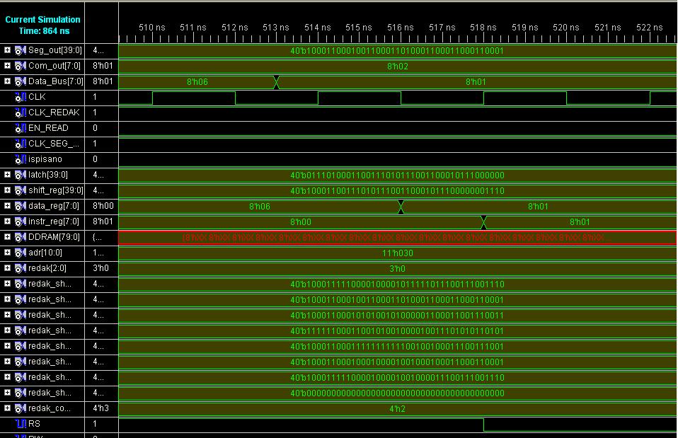
I have a project on my universty, my team needs to program the WHOLE HD44780 LCD controller in Verilog on Xilinx Spartan 3e.

We are begginers in FPGA modeling in Verilog, so it's pretty hard for us to even start. Good thing in this project is that we can use a already writing code, but we need to explain it line by line.. :)

We found the interfacing of HD44780, but that's not the problem, we need to implement the whole core, a bit simplified. In HD44780 datasheet
https://www.sparkfun.com/datasheets/LCD/HD44780.pdf
the block diagram is not so readble, not to us. Biggest problems are CGROM, DDRAM, SEG and COM signals..

We can you use similar controller also, practicly they are all on the same basis

I googled the whole net, nothing, except interfacing, of which we have no use...

If anyone can help or if anyone has a project done it would be nice.. :)

Greeting from Croatia, Split! ;)
 

HD44780 fpga core

I think the question title is misleading, you apparently mean interfacing the HD44780 in Verilog, not implementing it? If the project possibly implies designing a HD44780 model for test purposes (you don't clearly tell about this point), it can only apply to the digital part (bus interface and controller) not the analog part (LCD driver). The latter can't be represented by a digital HDL.
 

    Defton

    Points: 2
    Helpful Answer Positive Rating
Re: HD44780 fpga core

If the project possibly implies designing a HD44780 model for test purposes (you don't clearly tell about this point), it can only apply to the digital part (bus interface and controller) not the analog part (LCD driver).

Right, i wasn't clear enough, my bad.

We need to make all of this in Verilog:

**broken link removed**
 

HD44780 fpga core

May I ask, what's the purpose of implementing the HD44780 controller in FPGA? As said, the common signal and segment signal driver involves special analog cells and can't be implemented in FPGA.
 

Re: HD44780 fpga core

Tell that to my professor. ;)

No purpose. We will probably connect the LCD panel on FPGA to try if it works.
So it is not possible?
 

HD44780 fpga core

What type of LCD panel do you want to connect?
 

    Defton

    Points: 2
    Helpful Answer Positive Rating
Re: HD44780 fpga core

My interpretation of your request is that the professor would like you to demonstrate a circuit which demonstrates two asynchronous interfaces: an LCD interface which is clocked at nice regular intervals, and a CPU interface which is clocked whenever the host CPU feels like it. From what I can tell of the 'real' chip, the two interfaces aren't fully asynchronous; commands which arrive asynchronously from the host CPU will be latched asynchronously, but processed synchronously with the LCD scanning.

I'm not sure the common LCD controllers are the best sort of project for practicing CPLD/FPGA design, since they do have a few quirks. Still, it shouldn't be too hard to cobble things together to test the FPGA with real display drivers (most LCD panels shift four bits of data at a time, so character spacing would probably have to be pushed to 8 pixels instead of 6, but that shouldn't be a problem).

An interesting aspect of this design might be the design of an efficient "RAM", given common FPGA building blocks. If in the part you are using a flip-flop with a single input is "cheaper" than anything more complicated, an optimal design may end up holding display data using lots of shift registers. Trying to put all 960 bits of display data into a single shifter would probably not be a good idea (outputting one scan line of a character to the LCD would require cycling through all 960 bits; outputting one scan line of a 40-character row would require 38,400 shifts) but it may be useful to store character data as eight 80-bit shift registers (each shift would expose one byte from each of the 80 characters, stored alternately for the first and second line); shape data could be stored as eight groups of five 8-bit shifters (one group for each custom character, and one shifter per column).

Using an approach like that would minimize the amount of circuitry required for display addressing. Display updates would be somewhat slow, since the main CPU interface would be unable to write display data until it "rolled around", but that shouldn't be too bad (one would probably want to add 7 extra clocks per scan line to "roll" the character data through the shifter and give the CPU interface a chance to update it.
 

    Defton

    Points: 2
    Helpful Answer Positive Rating
Re: HD44780 fpga core

@FvM

I asked my professor yesterday, what are we really trying to make. He respond that we are going to TRY to make the HD44780 with everything, cause it's a industry standard and it can't be found in parts, control chip an LCD. It's a challenge he said.
Also i asked him about the analog parts you mentioned, we will do them analog. :)

First we need to figure out the how are signs displayed on LCD with common and segment signals, it's necessary so understand the timing diagram. We have problem with that cause the HD44780 datasheet is not complete.

Second, it's about clocks. I did some code by myself, but i'ts a problem cause in the block diagram some parts are not complete, BUS are not marked correct, and datasheet doesn't explain the function of TIMING GENERATOR, PARRALEL/SERIAL CONVERTER, 40 bit Shift Reg (SEGMENT), 40bit latch circuit, 16bit shiftregistar(COMMON), COM and SEG drivers, Cursor and blink control, etc..


@super

Thank you very much.

Pardon me about my bad english, the technology english isn't my good side... :)
 

Re: HD44780 fpga core

A datasheet is not intended as a chip construction manual. You possibly need to search for additional literature (hardware manuals of similar chips, applications notes, LCD glass specifications). Some points, e.g. drive waveforms can be determined by measurements.

All in all, it's feasible to assemble a working LCD controller with similar properties as HD44780. Building the analog part separate to a FPGA based digital part is possible of course, but implies a lot of transistors or analog switches.

Larger displays are utilizing extension drivers supplementing the HD44780 (the function of the respective pins is only briefly mentioned in the datasheet. If you can get suitable segment drivers, you can use them also in place of the HD44780 build-in segment drivers. See below datasheet of a newer LCD controller and extension driver for reference.
 

Re: HD44780 fpga core

If you're trying to emulate the 44780 interface to the CPU-interface level, there are a variety of approaches you can take. As I noted above, using shift registers for a lot of things will probably help minimize the amount of logic required. Do you have any idea what speed clock you can get away with? If you're using a 5MHz clock, that will allow a command to take 200 clock cycles and still meet the datasheet spec of 40us. If you're shifting one pixel per clock, shifting a 40-character-wide display will use up all your clocks without leaving any available for CPU access unless you split the shifting of each line into multiple sub-operations (which might actually not be a bad idea, but would somewhat complicate the logic).
 

HD44780 fpga core

It's not obvious, which timing restriction you're referring to. HD44780 is actually using a low frequency(< 500 kHz) clock,
that is split into mutiple phases, but no further internal parallelization, as far as I'm aware of.
 

Re: HD44780 fpga core

Ok, thanx for help.

Can u help me to start?

I started writing the code.
What i got here is this..
Please condsider that i'm a total noob in this so.. :)

Code:
`timescale 1ns / 1ps

module HD44780(RS, RW, E, DB, DB1);
		//MPU Interface
		input RS, RW, E; //
		input [7:0]DB1;
		output [7:0]DB;
	// When RS = 0 and R/W = 1 (Table 1), the busy flag is output to DB7.
		
		reg[7:0]DB;
		
		wire [6:0]IR_AC;
		wire [6:0]AC_DD_DB;
		wire [7:0]DD_CG;
		wire [7:0]DR_CG;
		wire [4:0]CG_PSC;
		wire [7:0]TG_DDR;
		
		
		//moduli
		Data_Reg DR(.DR_input(DB), .RS(RS), .RW(RW), .DR_output(DR_DD), .CLK(E));
		Inst_Reg IR(.IR_input(DB),  .IR_out(IR_AC),.CLK(E), .RS(RS), .RW(RW));
		Adr_count AC(.Adr_in(IR_AC),.Adr_out(AC_DD_DB), .CLK(E), .RS(RS), .RW(RW)); //The AC contents are then output to DB0 to DB6 when RS = 0 and R/W = 1 (Table 1).
		DDRAM DD(.Adr_in(AC_DD_DB), .DDR_out(DD_CG), .DR_in(DR_DD), .TG_in(TG_DDR), .CLK(E), .CLK_RW(RW));
		CGROM CG(.DDR_out(DD_CG), .CLK(E), .DDR_in_adr(DR_DD), .PSC_out(CG_PSC));
		Timing_Generator TG(.TG_out(TG_DDR));
		
		always@(DB1) DB=DB1;
		
endmodule

module Data_Reg(DR_input, DR_output, CLK, RS, RW); //Data registar
		
		input[7:0]DR_input;
		output[7:0]DR_output;
		input CLK, RS, RW;
		
endmodule

module Inst_Reg(IR_input,IR_out, CLK, RS, RW);
		
		input[7:0]IR_input;
		input CLK, RS, RW;
		output [6:0]IR_out;

		reg [6:0]IR_out;
		
		always@(posedge CLK)
			begin
				if(RS==0 && RW==0)
						begin
							if(IR_input == 8'b0000001)
									IR_out = 7'h20;// clear display
							/*if(IR_input == 8'b000001z)//return home
							if(IR_input == 8'b0000100)// samo dekremenitiraj
							if(IR_input == 8'b0000101)// dekremenitiraj i shiftaj
							if(IR_input == 8'b0000110)// samo inkrementiraj
							if(IR_input == 8'b0000111)// inkremenitiraj i shiftaj
							if(IR_input == 8'b0001000)// display off
							if(IR_input == 8'b0001111)// display on, cursor i blinkaj je on
							if(IR_input == 8'b00111zz)// display shift, pomakni desno
							if(IR_input == 8'b00110zz)// display shift, pomakni livo
							if(IR_input == 8'b00100zz)// UGASI shift, pomakni livo
							if(IR_input == 8'b00100zz)// UGASI shift, pomakni DESNO
							if(IR_input == 8'b01100zz)// odabir 8, 5*8 slova, jedna linija itd.*/
						end
				end
		
		reg [7:0]inst_reg;
		always @(posedge CLK)
			inst_reg = IR_input; //spremi trenutnu naredbu koju dobij
		
endmodule

module Adr_count(Adr_out, Adr_in, CLK, RS, RW);
		
		input [6:0]Adr_in;
		input CLK, RS, RW;
		output[6:0]Adr_out;
		
		reg[6:0]Adr_out;
		
		reg[6:0]AC;
		
		always @(CLK) AC <= 0;
		always@(Adr_in)
					begin
							AC <= AC + 1'b1; //kad primi¹ adresu za DDRAM uveæaj za 1
							Adr_out = Adr_in;
							if(Adr_in==6'h20) 
								begin
									AC <= 0; //za funciju clear display
									Adr_out = Adr_in;
								end
				    end
		
endmodule


module DDRAM(Adr_in, DDR_out,DR_in, TG_in, CLK_RW, CLK);// treba sinkronizirati ovos ve
		
		input [7:0]Adr_in, TG_in, DR_in;
		input CLK, CLK_RW;
		output [7:0]DDR_out;
		
		reg [7:0]DDR_out;
		
		reg [7:0] mem[79:0]; //velièina memorije
		
		always@(Adr_in)
		begin
			if(CLK_RW == 1) 
			begin
				mem[Adr_in] = Adr_in;
			end
			else if(CLK_RW == 0)
			begin
				DDR_out = mem[Adr_in];
			end
		end		
	
		
endmodule
	
module CGROM(DDR_in_adr, DDR_out, PSC_out, en_read, CLK);
			
			input [7:0] DDR_in_adr;//ulaz
			input en_read,CLK;//
			
			output[7:0] DDR_out;
			output[4:0] PSC_out;// izlaz - paralelno serijski konverter
			
			reg [4:0] mem [1983:0];
			
			// memorija velièine 9920 bita
					mem[1]=0;
					mem[9]=5'h11;//H
					mem[10]=5'h11;
					mem[11]=5'h11;
					mem[12]=5'h1F;
					mem[13]=5'h11;
					mem[14]=5'h11;
					mem[15]=5'h11;
					mem[16]=5'h00;
					mem[17]=5'h1E;//D			
					mem[18]=5'h11;
					mem[19]=5'h11;
					mem[20]=5'h11;
					mem[21]=5'h11;
					mem[22]=5'h11;
					mem[23]=5'h1E;
					mem[24]=5'h00;
					mem[25]=5'h02;//4
					mem[26]=5'h06;
					mem[27]=5'h0A;
					mem[28]=5'h12;
					mem[29]=5'h1F;
					mem[30]=5'h02;
					mem[31]=5'h02;
					mem[32]=5'h00;
					mem[33]=5'h02;//4
					mem[34]=5'h06;
					mem[35]=5'h0A;
					mem[36]=5'h12;
					mem[37]=5'h1F;
					mem[38]=5'h02;
					mem[39]=5'h02;
					mem[40]=5'h00;
					mem[41]=5'h1F;//7
					mem[42]=5'h11;
					mem[43]=5'h01;
					mem[44]=5'h02;
					mem[45]=5'h04;
					mem[46]=5'h08;
					mem[47]=5'h08;
					mem[48]=5'h00;
					mem[49]=5'h0E;//8
					mem[50]=5'h11;
					mem[51]=5'h11;
					mem[52]=5'h0E;
					mem[53]=5'h11;
					mem[54]=5'h11;
					mem[55]=5'h0E;
					mem[56]=5'h00;
					mem[57]=5'h0E;//0
					mem[58]=5'h11;
					mem[59]=5'h13;
					mem[60]=5'h15;
					mem[61]=5'h19;
					mem[62]=5'h11;
					mem[63]=5'h0E;
					mem[64]=5'h00;
endmodule
	
 module Timing_Generator(TG_out_40, TG_out_16, TG_out);
		output [6:0]TG_out_40;
		output [3:0]TG_out_16;
		output [6:0]TG_out;		
				
endmodule
 

Re: HD44780 fpga core

Defton said:
Can u help me to start?

The 44780 does not require data to be valid until the falling edge of E, so you shouldn't latch it until then. It does require the address and r/w to be valid prior to the rising edge, but since they are also required to remain valid until the falling edge, it's probably easiest to latch everything on the falling edge of E, except for the data bus output-enable and output data, which you could generate combinatorially (If R/W is asserted late, data will be output on the bus until a small prop delay after it's asserted; if it's deasserted late, data won't be output until a small prop delay after it's deasserted. If the address is set late, data won't be valid until a small prop delay after it's set. If the host system doesn't mind such behavior, the display controller shouldn't care either).

Also, it looks as though you're trying to write the display address to display RAM, rather than writing the data.
 

Re: HD44780 fpga core

Impossible, it's hard, we cant do it without precise details in datasheet.. :(
 

Re: HD44780 fpga core

Defton said:
Impossible, it's hard, we cant do it without precise details in datasheet.. :(

What particular information do you need? Timings given in data sheets are worst-case rather than expected (and might vary somewhat between different chips anyway) but if you make something that conforms to the worst-case timing, that should suffice.
 

Re: HD44780 fpga core

we cant do it without precise details in datasheet
As I already mentioned: "A datasheet is not intended as a chip construction manual." I fear, you basically have to re-invent the chip for your project, I don't think that you'll find functional or even synthesizable HDL code for it. But I'm almost confident, that the prject can be done.
 

Re: HD44780 fpga core

FvM said:
we cant do it without precise details in datasheet
I fear, you basically have to re-invent the chip for your project, I don't think that you'll find functional or even synthesizable HDL code for it. But I'm almost confident, that the prject can be done.

It would be necessary to re-engineer much of the chip. Given the relatively relaxed timing of much of it, it probably shouldn't be too hard to do so.

If you'd rather design your own display system, I'd suggest the following as a challenge:

-1- Drive a 256x64 display, using a 1024x16 single-ported RAM, using a clock of 400KHz or less (faster clocks would use more power).

-2- Allow a remote CPU to access the display as fast as it wants using an 8-bit bus, up to the maximum access speed of the RAM, with no minimum bus speed or maximum transaction time (changing address would be a separate operation from reading or writing data). Allow some means of performing read-modify-write.

The tricky part here would be coming up with a good clock to drive the display-memory logic to avoid feeding any 'runt' accesses to the display. If the CPU is actively reading or writing memory, its read-write signals can be used to generate a clock twice as fast as the rate at which the 16-bit memory will have to be read or written, but the RAM would have to be clocked for display refresh even when the CPU wasn't accessing it.
 

Re: HD44780 fpga core

Guys, i've done this so far...
i'ts on croatian, so maybe it will be hard to understand,
but you will probably figure it out!

Code:
module HD44780(
			RS,
			RW,
			E, 
			Seg_out,
			Com_out,
			Data_Bus, 
			CLK, CLK_REDAK, 
			EN_READ, 
			CLK_SEG_OUT);
		
		input 
		RS, //mpu
		RW, //mpu
		E,  //mpu
		CLK, 
		CLK_REDAK, 
		EN_READ,
		CLK_SEG_OUT;

		//taktni signali
		input [7:0]Data_Bus;//ulazne naredbe 8bitne;
		output[39:0]Seg_out;//segmetni signali - stupci
		output[7:0]Com_out;//common signali - redci
		
		reg[39:0]Seg_out;
		//reg[7:0]Com_out;

		//reg[7:0]Adresa_znaka;
		//reg[2:0]Adresa_retka;
		reg[7:0]data_reg;//podatkovni registar
		reg[7:0]instr_reg;//instrukcijski registar
		reg[39:0]shift_reg;//shift registar za segmente signale
		reg[39:0]latch;//latch koji sprema sadr¾aj shift registra za seg_signale
		// reg[7:0]shift_reg8;
		reg[2:0]Adress_counter;
		
		reg Busy_Flag;
		
		initial instr_reg = 0;
	
		/////DEFINIRANJE INTRUKCIJA//////
		always@(posedge E or RS or RW)
			begin
				if(RS==0 && RW ==0)
					begin
					instr_reg = Data_Bus;
					
					end
				end	
		
		/////////DDRAM////////////////
		reg [7:0] DDRAM[79:0]; 
		
		
		///////CGROM/////////
		reg [4:0] mem [55:0];
			
			always@(CLK)
				begin
					mem[0]=5'h00;//space
					mem[1]=5'h00;	
					mem[2]=5'h00;	
					mem[3]=5'h00;	
					mem[4]=5'h00;	
					mem[5]=5'h00;	
					mem[6]=5'h00;	
					mem[7]=5'h00;	
					mem[8]=5'h11;//H
					mem[9]=5'h11;
					mem[10]=5'h11;
					mem[11]=5'h1F;
					mem[12]=5'h11;
					mem[13]=5'h11;
					mem[14]=5'h11;
					mem[15]=5'h00;
					mem[16]=5'h1E;//D			
					mem[17]=5'h11;
					mem[18]=5'h11;
					mem[19]=5'h11;
					mem[20]=5'h11;
					mem[21]=5'h11;
					mem[22]=5'h1E;
					mem[23]=5'h00;
					mem[24]=5'h02;//4
					mem[25]=5'h06;
					mem[26]=5'h0A;
					mem[27]=5'h12;
					mem[28]=5'h1F;
					mem[29]=5'h02;
					mem[30]=5'h02;
					mem[31]=5'h00;
					mem[32]=5'h1F;//7
					mem[33]=5'h11;
					mem[34]=5'h01;
					mem[35]=5'h02;
					mem[36]=5'h04;
					mem[37]=5'h08;
					mem[38]=5'h08;
					mem[39]=5'h00;
					mem[40]=5'h0E;//8
					mem[41]=5'h11;
					mem[42]=5'h11;
					mem[43]=5'h0E;
					mem[44]=5'h11;
					mem[45]=5'h11;
					mem[46]=5'h0E;
					mem[47]=5'h00;
					mem[48]=5'h0E;//0
					mem[49]=5'h11;
					mem[50]=5'h13;
					mem[51]=5'h15;
					mem[52]=5'h19;
					mem[53]=5'h11;
					mem[54]=5'h0E;
					mem[55]=5'h00;
						
			end
			
	////////ZA CITANJE IZ CGROM-a//////////
			reg[10:0]adr;
			reg[2:0]redak;
			reg ispisano;
			
			
		reg[39:0]redak_shift0;
		reg[39:0]redak_shift1;
		reg[39:0]redak_shift2;
		reg[39:0]redak_shift3;
		reg[39:0]redak_shift4;
		reg[39:0]redak_shift5;
		reg[39:0]redak_shift6;
		reg[39:0]redak_shift7;
		
			integer i; 
			always@(negedge CLK)
				begin
				if(instr_reg==0 && RS == 1 && RW ==0)
					begin
					data_reg=Data_Bus;
					DDRAM[data_reg] = data_reg;
					end
				if(instr_reg == 8'b00000001 && RS==1 && RW == 0)
						begin
						for(i=1; i<=8;i=i+1)
							begin
							data_reg = 8'h00;
							end
						Busy_Flag = 1;
						DDRAM[data_reg] = data_reg;
						end
				
				if(EN_READ == 1 && ispisano == 0)
				begin
					adr ={data_reg,redak};
					shift_reg=shift_reg<<5;
					shift_reg[4:0]= mem[adr];		
					
					if(redak == 3'b111)
					 begin
						ispisano = 1;
						redak = 3'b000;
						
					 end
					 else
						redak =redak + 1;
	
				end
				else
				begin
					ispisano=0;
					redak=0;
				end
			end
			
			always@(ispisano)
			begin
				if (ispisano==1)
					latch = shift_reg;
			end
			
			always@(posedge CLK_REDAK)
				begin
					if(CLK_REDAK==1);
						begin
								redak_shift0 = redak_shift0<<5 ;
								redak_shift1 = redak_shift1<<5 ;
								redak_shift2 = redak_shift2<<5 ;
								redak_shift3 = redak_shift3<<5 ;
								redak_shift4 = redak_shift4<<5 ;
								redak_shift5 = redak_shift5<<5 ;
								redak_shift6 = redak_shift6<<5 ;
								redak_shift7 = redak_shift7<<5;
								
								redak_shift0[4:0] = latch[39:35];
								redak_shift1[4:0] = latch[34:30];
								redak_shift2[4:0] = latch[29:25];
								redak_shift3[4:0] = latch[24:20];
								redak_shift4[4:0] = latch[19:15];
								redak_shift5[4:0] = latch[14:10];
								redak_shift6[4:0] = latch[9:5];
								redak_shift7[4:0] = latch[4:0];
								
		
						end
				end
			
			reg[3:0]redak_counter;//broojaè redak za COM Signale... 
			
			assign Com_out = (Seg_out == redak_shift0)? 8'b00000001:// com_demux_
								  (Seg_out == redak_shift1)? 8'b00000010:
								  (Seg_out == redak_shift2)? 8'b00000100:
								  (Seg_out == redak_shift3)? 8'b00001000:
								  (Seg_out == redak_shift4)? 8'b00010000:
								  (Seg_out == redak_shift5)? 8'b00100000:
								  (Seg_out == redak_shift6)? 8'b01000000: 8'b10000000;
								  
			initial redak_counter = 0;
			always@(posedge CLK_SEG_OUT)
			begin
				if(CLK_SEG_OUT == 1 && redak_counter == 0)
					begin
					Seg_out = redak_shift0;
				   redak_counter = redak_counter + 1;
					end
			   else if(CLK_SEG_OUT == 1 && redak_counter == 1)
					begin
					Seg_out = redak_shift1;
					redak_counter = redak_counter + 1;
					end					
				else if(CLK_SEG_OUT == 1 && redak_counter == 2)
					begin
					Seg_out = redak_shift2;
					redak_counter = redak_counter + 1;
					end
				else if(CLK_SEG_OUT == 1 && redak_counter == 3)
					begin
					Seg_out = redak_shift3;
					redak_counter = redak_counter + 1;	
					end
				else if(CLK_SEG_OUT == 1 && redak_counter == 4)
					begin
					Seg_out = redak_shift4;
					redak_counter = redak_counter + 1;	
					end
				else if(CLK_SEG_OUT == 1 && redak_counter == 5)
					begin
					Seg_out = redak_shift5;
					redak_counter = redak_counter + 1;
					end
				else if(CLK_SEG_OUT == 1 && redak_counter == 6)
					begin
					Seg_out = redak_shift6;
					redak_counter = redak_counter + 1;	
					end
				else if(CLK_SEG_OUT == 1 && redak_counter == 7)
					begin
					Seg_out = redak_shift7;
					redak_counter = 0;
					end	
			 
			
			//redak_counter=redak_counter + 1;
			end
			//Adress_Co1unter
	endmodule

this is what i've and it gives this on output, if you look hard you can see the output HD44780 on redakshift registers ;) :
 

Re: HD44780 fpga core

Good news!

I've done the similiar controller and it works!
Now, the professor is asking to do the same on ADSP-BF533 EZ-KIT Lite®!

He said that we need try to simulate the same thing, example-to send 40bits over SPORT interface or SPI.

So, help anyone?
I'm buying a pizza! ;)
 

Status
Not open for further replies.

Part and Inventory Search

Welcome to EDABoard.com

Sponsor

Back
Top