Continue to Site

Welcome to EDAboard.com

Welcome to our site! EDAboard.com is an international Electronics Discussion Forum focused on EDA software, circuits, schematics, books, theory, papers, asic, pld, 8051, DSP, Network, RF, Analog Design, PCB, Service Manuals... and a whole lot more! To participate you need to register. Registration is free. Click here to register now.

Opamp circuit for ADC input

Status
Not open for further replies.

Tom-nor

Newbie level 6
Joined
Jan 22, 2010
Messages
14
Helped
0
Reputation
0
Reaction score
0
Trophy points
1,281
Location
Norway
Activity points
1,409
Hey guys!

Would be awsome if anyone pls could take a quick look at my problem.

Got a +- 300 mV input singal comming from a piezo electric sensor.

My ADC works in the range 0-2.8 V.

So iam gna bias the input signal with 1 volt. I need to take advantage of the opamps high input impedance, so i have conected the inputsignal trough a capacitor and to the opamps + input.

But iam having slight problems with how to connect the voltage divider to bias the signal, without messing up the amplifying ( which i want to be 1) or the input impedance.

I got a single 12 volt power suply.

Thnx for your time, i hope the info i have given you is enough and i apologize for my english.

Regards: Tom
 

If you don't insist on (exactly) gain=1 , you could insert a feedback voltage divider of 0.4 : 1 (e.g. 39kΩ : 100kΩ) between output and GND and connect the tap of the divider to the inverting input. Thus you have an input bias of 1V at the opAmp inputs, 1.4V at its output (the center point of your ADC input range), and a voltage gain of 1.4 .
 

    Tom-nor

    Points: 2
    Helpful Answer Positive Rating
Ok bro, ill try that. thnx heaps!

Never used a voltage divider at the opamp output before, but then again, im no expert :)

Added after 1 hours 46 minutes:

Something likes this you had in mind?

when i simulate this, the center point is around 2.8 volts. which is a bit high, and i cant seem to lower it by changing resistor values.


if i hook up a cap at the output, it varies from 0 and up, which looks good but then i dont know where the actual 0v of the original signal lies.

Again, sry for being a noob lol. Not rly my field of knowledge :)[/img]
 

Tom-nor said:
Something likes this you had in mind?
Exactly.

Tom-nor said:
when i simulate this, the center point is around 2.8 volts. which is a bit high, and i cant
With a 356 type opAmp this cannot work, because a voltage range of 0 ... 3V doesn't lie within the input common voltage range of these amplifiers. You should use a GND-input-capable opAmp like the LM324 / LM2902 . If you use a different type, look for a specification saying "Input common-mode voltage range includes ground".
 

Hey, again thnx for your help!

checked out the datasheet for LM324 / LM2902, but i think theres an issue with the input voltage range. its says that -0.3 volts on the input is as low as it goes before the output goes to V+.


Does that go for an AC signal?, or is it -0.3 dc ?

And my input signal is as mentioned about +- 300mv.

So my simulation is still not working as expected, so i raised the input pulse signal im using to -200 mv to 400 mv and still not working.

So not sure if its the opamp, or if im doing something else wrong. Maby a pulse generator isent they way to go when i simmulate.
 

Tom-nor said:
checked out the datasheet for LM324 / LM2902, but i think theres an issue with the input voltage range. its says that -0.3 volts on the input is as low as it goes before the output goes to V+.
No, this means the input common voltage range goes down even to -0.3V, which means it can accept input voltages up to -300mV and still works well.

Tom-nor said:
Does that go for an AC signal?, or is it -0.3 dc ?
Would be ok for both DC and AC. But you wanted to bias the input with 1 volt, that's how I designed the feedback network.

Tom-nor said:
And my input signal is as mentioned about +- 300mv.
Sure, but you insert it via AC coupling (the 10nF cap), hence no DC part will be transferred to the opAmp.

Tom-nor said:
So my simulation is still not working as expected, so i raised the input pulse signal im using to -200 mv to 400 mv and still not working.
What are the DC voltages at the inputs and on the output of the LM324 ? Do they show the voltages which I indicated?

Tom-nor said:
So not sure if its the opamp, or if im doing something else wrong. Maby a pulse generator isent they way to go when i simmulate.
Could you post your schematic with the DC bias voltages, and perhaps your simulation schematic?
 

    Tom-nor

    Points: 2
    Helpful Answer Positive Rating
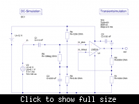
Heres pics of voltage at opamp output, and inverting input.

Maby i missunderstood then concept of biasing, and that i need to add some more to my circuit?
 

Think i can use this circuit (follower), if i can find a suitable opamp.
Singly suply. and very high input impendance.

The 324 opamp works well when i use resistors 20k and 220k, but i need to able to use way larger resistors. 2M and 22M or even higher.

Its abit hard to find a suitable one that runs on singlesupply tho, but gna look into it.
Not sure if this is the easiest way to do it tho.

what do you think?

thnx for taking the time to assist me on this!
 

Tom-nor said:
Maby i missunderstood then concept of biasing, and that i need to add some more to my circuit?
Sorry, Tom,
this was my error :-(. The input bias is not defined, that's why your output is changing with time. The non-inverting input must receive an input bias - as you did in your circuit follower.jpg, but you can provide this bias via a (very) high-ohmic resistor, in order not to load your input source too much. See the following schematic:
A few notes:
  • In order to use the full ADC input range, I suggest to use some gain. With a gain of (1 + R2/R1) = 4.3 (s. schematic) you can amplify the ±300mV input signal to about ±1.3V , which would use nearly the full input range of your ADC
  • I'd suggest to use a 5kΩ potentiometer instead of R3, in order to adjust the opAmp's quiescent output voltage to the mid voltage of the ADC, i.e. to 1.4V .
  • C3 should filter the inverting input's bias voltage to get it free of noise and line ripple. Use a capacitance between 100 .. 1000µF (Minus to GND).
  • C2 is a filter cap for the opAmp's power supply. Should be as close as possible at the opAmp's power supply inputs.
Tom-nor said:
Its abit hard to find a suitable one that runs on singlesupply tho, but gna look into it.
If you find a single supply (or a rail-to-rail) opAmp (input common mode range includes 0 Volt = GND is necessary!) with either jFET or MOSFET inputs, you may increase R5 two orders of magnitude (1GΩ) if this should be necessary for your input source.
 

    Tom-nor

    Points: 2
    Helpful Answer Positive Rating
Tom-nor said:
Think i can use this circuit (follower), if i can find a suitable opamp.
Singly suply. and very high input impendance.

The 324 opamp works well when i use resistors 20k and 220k, but i need to able to use way larger resistors. 2M and 22M or even higher.

Its abit hard to find a suitable one that runs on singlesupply tho, but gna look into it.
Not sure if this is the easiest way to do it tho.

what do you think?

thnx for taking the time to assist me on this!

Checkout the TLV2262 from TI, it works for both single supply, rail to rail and I think you can request free samples from TI...
 

    Tom-nor

    Points: 2
    Helpful Answer Positive Rating
adinogcas said:
Checkout the TLV2262 from TI, it works for both single supply, rail to rail and I think you can request free samples from TI...
Yes, this one is well appropriate for R5=1GΩ, however not for a supply voltage of 12V, because its power supply voltage is limited to 8V. I'd recommend to supply it with 5V (and then reduce R4 to 47kΩ).
 

    Tom-nor

    Points: 2
    Helpful Answer Positive Rating
Awsome stuff guys! Thnx alot!

Did not have time today to check it all out, but gna try to take some time tommorow.

And yeah, deffinatly going for a fet input oppamp.

Anyways, ill post my progress when i have more time.

thnx again, have a great weekend

Regards: Tom
 

Been doing some simulations with the LM324 now, with a +-250mV input signal.
Seems to me that this opamp cant handle the 10Meg resistor at the input, not sure.

the input bias current is typ 45nA. 45nA * 10Meg = 0.45 V of extra input.
Maby thats the point, not very steady on this stuff, just thinking out loud :)

I have uploaded pictures of with the values 10Meg and 100k for this resistor.
As you can see the 100k is more in the "correct" area, altough the output is ugly.

So i tried with the 10Meg resistor again, but switched the feedback gain from 3.3 to 1.
Wont the 1 V input bias be amplified with a factor of 3.3 aswell??

With the feedback gain `= 1 it looks ok.

or maby just my simulations is wrong. Anyways thnx for your help again.

Gna try with the TLV2262 now and see how that works out.
 

Ok, here is the same simulations with the tlv2262, looks abit better

And i should add to the simulations before, the opamp settles at more expected values after a short time. Say i put start time 50ms and end time 60ms, instead of 0 and 10ms. The output is completely different.

So that kinda got me fooled abit, so not sure how everything is gna work when i make a prototyp. But im going for the lmv2262 due to its mosfet input.
And i think your recomendation of a potmeter instead of the 3.3 k omh resistor is a very good idea.

So gna try to get the opamp ordered, and start working on blocking negativ voltage and voltage over 2.8V after the opamp output. Dont wanna kill my adc :)
If i remember correctly, you can block negative voltages with a diode, and block the voltages higher than 2.8 V with a zener?
 

Tom-nor said:
the input bias current is typ 45nA. 45nA * 10Meg = 0.45 V of extra input.
You can quite well compensate the input bias current influence by inserting another resistor with the same value (10Meg) between the feedback node and the inverting input.

Tom-nor said:
So i tried with the 10Meg resistor again, but switched the feedback gain from 3.3 to 1. ... With the feedback gain = 1 it looks ok.
This was with gain = 1 + R2/R1 = 2 , not 1 !

Tom-nor said:
Wont the 1 V input bias be amplified with a factor of 3.3 aswell??
Sure; that's why I designed the input bias to be 1.4V/4.3 ≈ 325mV . 12V * 3.3k/123.3k = 321mV .

Tom-nor said:
Ok, here is the same simulations with the tlv2262, looks abit better

And i should add to the simulations before, the opamp settles at more expected values after a short time. Say i put start time 50ms and end time 60ms, instead of 0 and 10ms. The output is completely different.

So that kinda got me fooled abit, so not sure how everything is gna work when i make a prototyp.
Don't panic ;-) Your input RC time constant is 1e7 * 1e-8 = 100ms. It takes about 3 time constants to load the 10nF to ≈90% of its final operating point, a very long time for your simulation (unless you put the correct initial value on your cap, resp. on the inp node), but nothing in reality ;-)

Tom-nor said:
But im going for the lmv2262 due to its mosfet input.
Good decision!

Tom-nor said:
And i think your recomendation of a potmeter instead of the 3.3 k omh resistor is a very good idea.
Then you can adjust your quiescent output voltage.

Tom-nor said:
So gna try to get the opamp ordered, and start working on blocking negativ voltage and voltage over 2.8V after the opamp output. Dont wanna kill my adc Smile
If i remember correctly, you can block negative voltages with a diode, and block the voltages higher than 2.8 V with a zener?
I'd suggest to block with 2 diodes against 0V and 2.8V . A 3V zener has a rather soft breakdown voltage - unlike >5V diodes, which also are called zeners, but in reality are avalanche diodes, thus show a steep breakdown behaviour. A 3V zener surely would ruin the accuracy of the upper voltage range.

Good luck! erikl
 

yeah lol, i ment A = 2, not 1, sry.

Thnx for all your help buddy, the oppamps should arrive some time this week, so abit on hold at the moment, ill keep posting once they arrive.

Regards: Tom
 

Got the opamps last week, made a small circuit bord so i can connect myselfs to the pins.

The circuit is working good, and almost rdy for the ADC input.

About the ADC protection, i figured i will supply the oppamp with 3.3 volts or smth to deny any higher output.

And about blocking the negative voltage, if i put a diode in series with the opamp output, and increase the bias with 0.35 ( 0.7 volts extra after amplification)
How will that affect my signal at the ADC input?

Regards: Tom
 

Tom-nor said:
About the ADC protection, i figured i will supply the oppamp with 3.3 volts or smth to deny any higher output.
You could do that, but not necessarily so. I'd recommend to use the same power supply as your ADC (or the µP which contains the ADC). For the overvoltage protection pls. s. below.

Tom-nor said:
And about blocking the negative voltage, if i put a diode in series with the opamp output, and increase the bias with 0.35 ( 0.7 volts extra after amplification)
How will that affect my signal at the ADC input?
A rather bad solution: this will deteriorate the accuracy of your signal resolution.

Better use a serial resistor from the output of the TLV2262 to the ADC input (should be much lower (at least a factor of 1000) than the input resistance of the ADC, which probably is quite high, so I think 10kΩ is a good value). Behind this series resistor (i.e. at the ADC input) use 2 protection diodes: one to GND (anode @ GND) and one to a "protection voltage" which should be the ADCs max. input voltage - 0.5V, i.e. about 2.3V (cathode @ 2.3V), this will limit the ADC input voltage to ≈2.9V which is tolerable, and will not deteriorate the accuracy of the upper signal range. Generate the 2.3V protection voltage by a voltage divider from the power supply, say with a 1 .. 5kΩ trim pot, incl. decoupling capacitor (10..100µF elko) from 2.3V to GND.

Use low-power diodes for this protection, something like 1N4148, not 1N400X types!

Good luck! erikl
 

    Tom-nor

    Points: 2
    Helpful Answer Positive Rating
Awsome stuff. Gna give that a go.

Cant rly say i understand the concept of a "protection voltage", but it will probably make more sense once i draw the circuit.

thnx for all of your help with this buddy.

tom
 

Hi again.

About to make a circuit board now, and a part of that is the oppamp circuitry we discussed above.

But i have to make 4 of them, becouse i got 4 different inputs.

Im looking to minizime the board, so im wondering if you could use the same "bias circuit" for all 4 Opamps, without damaging the effect.

Same question for the protection voltage aswell, is it enough with 1 cap and 8 diodes, or should i use 1 cap for every oppamp aswell?

Regards: Tom
 

Status
Not open for further replies.

Similar threads

Part and Inventory Search

Welcome to EDABoard.com

Sponsor

Back
Top