Continue to Site

Welcome to EDAboard.com

Welcome to our site! EDAboard.com is an international Electronics Discussion Forum focused on EDA software, circuits, schematics, books, theory, papers, asic, pld, 8051, DSP, Network, RF, Analog Design, PCB, Service Manuals... and a whole lot more! To participate you need to register. Registration is free. Click here to register now.

my problem with assura RCX

Status
Not open for further replies.

mightyocean

Newbie level 6
Joined
Mar 18, 2006
Messages
13
Helped
0
Reputation
0
Reaction score
0
Trophy points
1,281
Activity points
1,378
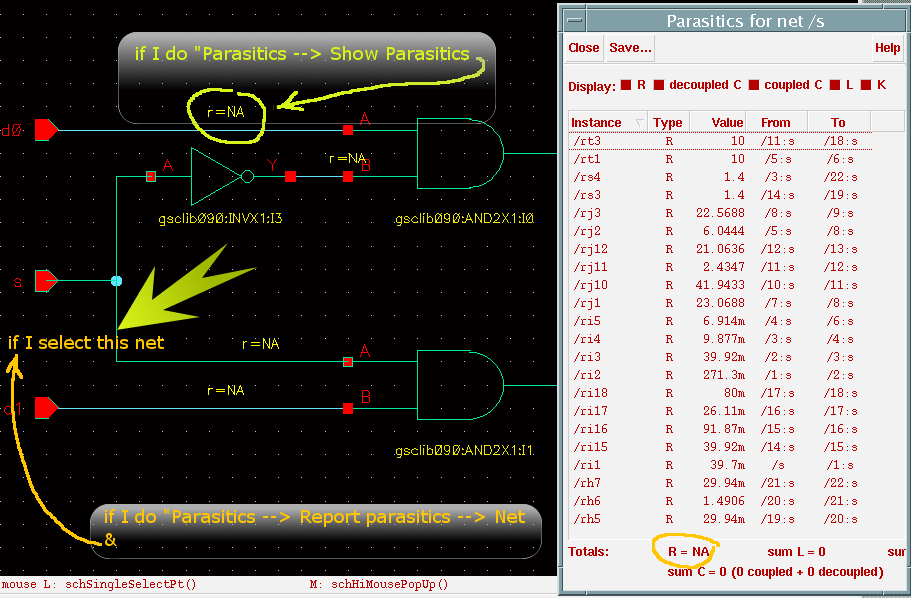
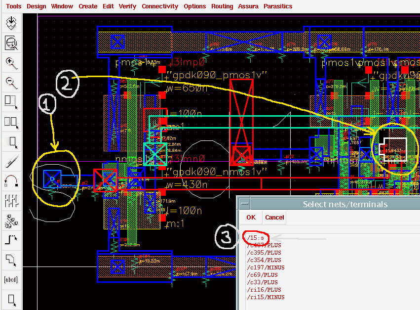
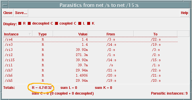
assura parasitic extraction fracture

hi,guys

These days I am doing a layout of a cascode amp,I set up vdd and gnd as inputoutput pins and label them in the layout.After I run a rcx to extract the RC parasitics,backannotate in the schematic and find that, the pcapacitors are displayed without the presistor, it showed "r=NA". But in the av_extracted view, I can see presistors by enlarging the layout. How can I figure this out? Thanks
 

assura rcx setup dir

You need to run a dc op-point sim for the resistors to correctly show-up
 

backannotate av_extracted view

hello, saro, could you show me how to do it?
I ran a dc sim,but don't know how to do next
 

In the schematic window go to Tools ->Parasitics. You must get a new menu added to the top named parasitics. Now Parasitics -> setup. Provide the path for the result directory. Then Parasitics -> show parasitics. Now you should be able to see the presistors.
I presume you are using cadence and ade.
 

There was a vague concept - called total-resistance for a net - in fact, people used such things before, without understanding - and ∑r for the whole net was made available [I am talking about history] by the tools then. Later as engineers understood - resistance is a point-to-point function, such ∑r was thing was kinda taken off - however still you want to see presistors that got extracted on the whole Net --> Menu Parasitics --> Report Parasitics --> Net [& select the Net]

See - Report Parasitics --> Net [purposely I did a R-Only extraction - to show you]
55_1226523376.png

https://obrazki.elektroda.pl/55_1226523376.png

Now, I'll say ∑r might make some sense - w.r.t. understanding/estimating RC delay in a path - from O/P of a gate to the input of another gate, if and only-if there is no branching in the net. In the branched net [net1] the total count of ∑r [that adds all the branches] does not make any sense for estimating delay between point-Y and point-A.
25_1226523546.png

https://obrazki.elektroda.pl/25_1226523546.png
In general lumped R for a Net has no meaning, sum R always makes sense from from point-to-point or, subNode-to-subNode in a same Net. As during parasitic extraction, each interconnect layer gets fractured into several pieces, and each piece represents a parasitic r&c - clicking on the schematic side does not make sense at all when user tries to get sumR between two points [schematic does not understand fracture or subnode of a net] - as say "Net1" on the layout/extracted is now fractured into several pieces - if you want to get R reporting - between a fracture to the other - this selection of subNode is possible only on the av_extracted view.

I'll upload couple of pictures to show - Parasitics --> Report Parasitics --> Terminal-to-Terminal. [under the mouse pointer where you click for selection of "first & second point", there can be several electrically connected layers - do select with common-sense]
23_1226523616.png

https://obrazki.elektroda.pl/23_1226523616.png

72_1226523692.png

https://obrazki.elektroda.pl/72_1226523692.png


Hope, it will help.
 

hi,saro,
I do exactly as you said before,and still got the "r=NA" results in the schematic. IN the CIW, it promts me to run a dc sim and supply the path to results by set up the Parasitics. I tried run a dc sim in ADE from both schematic and av_extracted, but neither changed the show-up.
Thank you all the same :D


saro_k_82 said:
In the schematic window go to Tools ->Parasitics. You must get a new menu added to the top named parasitics. Now Parasitics -> setup. Provide the path for the result directory. Then Parasitics -> show parasitics. Now you should be able to see the presistors.
I presume you are using cadence and ade.

Added after 4 minutes:

hi, sat
you don't know how grateful I am, your help really release me, I am confusinig for a couple of days. I need some time to digest your explanation.Thank you, thank you very much:D
 

Excellent Sat!..It's so nice of you to provide us with image illustrations.
I have a question.., If I ask parasitics -> report parasitics, it does report r the first time (or some times) and after that says NA, why does that happen? and can we depend on that value? (the value looks credible though)

I'm not able to select terminals in the av_extracted view! The entire layout area looks like a single block and I'm not able to make selections on it. Should I make terminals in the layout before doing this?(this does not make sense as it will add it's own res)
Will this allow me to see the resistances between any nodes or only between pins?

Thanks in advance,
Saro
 

Hi Saro,
Ah, you are not being able to select fractures on av_extracted is the same as I faced once.

I hope you know Layer Purpose Pair (LPP)

The reason is - shapes from LPP(Layer=Metal1,purpose=drawing[dg]) in the layout_view got translated into new (Layer=Metal1,purpose=Net[nt]) in the av_extracted view.

And - your Virtuoso LSW (Layer Selection Window), has been customized to have Metal1,purpose=Net
as NS (not Selectable)

Resolution:
LSW -->(Menu) Edit --> Set Valid Layers..

Make those Layers which carry nodal connectivity [like Poly, Metal1, Metal2,...] - "Visible" and "Selectable".
In the worst case - if cannot identify what, where - just make "All Valid"
 
hi,sat
my av_extracted view only display metal layer without any poly or other layer, is that the same problem as saro? I will try your method tomorrow
 

sat said:
Hi Saro,
Ah, you are not being able to select fractures on av_extracted is the same as I faced once.

I hope you know Layer Purpose Pair (LPP)

The reason is - shapes from LPP(Layer=Metal1,purpose=drawing[dg]) in the layout_view got translated into new (Layer=Metal1,purpose=Net[nt]) in the av_extracted view.

And - your Virtuoso LSW (Layer Selection Window), has been customized to have Metal1,purpose=Net
as NS (not Selectable)

Resolution:
LSW -->(Menu) Edit --> Set Valid Layers..

Make those Layers which carry nodal connectivity [like Poly, Metal1, Metal2,...] - "Visible" and "Selectable".
In the worst case - if cannot identify what, where - just make "All Valid"

That helped. Thanks a lot sat!.
 

Status
Not open for further replies.

Part and Inventory Search

Welcome to EDABoard.com

Sponsor

Back
Top