cyberrat
Advanced Member level 3
- Joined
- Jun 19, 2001
- Messages
- 902
- Helped
- 87
- Reputation
- 174
- Reaction score
- 43
- Trophy points
- 1,308
- Location
- In the sewers of the U.K.
- Activity points
- 5,900
Hello, can someone please advise me on what is good practise for the design of an RF transciever on a PCB.
Using 0603/0805 smt components on an 1.6mm 1oz FR4 board at 870mhz with groundplane underneath.
I would like to know things like.
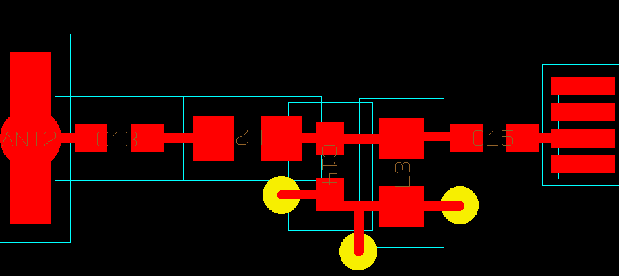
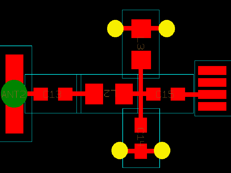
I.E. in the transmit line from an RF IC through the filters to the antenna, where I have a connection of
IC-C-LG-CG-L-C-ANT
IC= transciever IC
C=cap
L=inductor
LG=inductor to ground
CG=cap to ground
ANT=antenna. (Green dot on the left) (chip antenna)
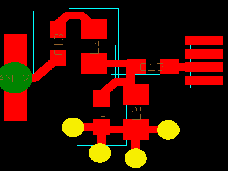
What would be the best way to lay the components out.
I.E.
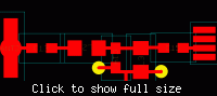
LAYOUT 1 - all in a line?
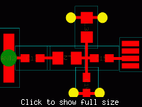
LAYOUT 2 - Split in cross fashion?
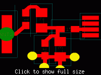
LAYOUT 3 - taking smallest board area up.
I can tell from the various books etc that layout 1 would be best however I would
prefer layout 3 as it takes less space.
Also should the L & C that go to ground be next to each other or are they OK as in layout 2?
As a newby to RF I would appreciate opinions from some that have experience of RF layout.
Thank you,
Roland
Added after 27 minutes:
Also, at the IC end, is it more important for the RF lines and components to be close to the PCB or the decoupling caps?
As there are VCC lines that when the cap is next to them make it so that the RF line cap is further away
Using 0603/0805 smt components on an 1.6mm 1oz FR4 board at 870mhz with groundplane underneath.
I would like to know things like.
I.E. in the transmit line from an RF IC through the filters to the antenna, where I have a connection of
IC-C-LG-CG-L-C-ANT
IC= transciever IC
C=cap
L=inductor
LG=inductor to ground
CG=cap to ground
ANT=antenna. (Green dot on the left) (chip antenna)
What would be the best way to lay the components out.
I.E.
LAYOUT 1 - all in a line?
LAYOUT 2 - Split in cross fashion?
LAYOUT 3 - taking smallest board area up.
I can tell from the various books etc that layout 1 would be best however I would
prefer layout 3 as it takes less space.
Also should the L & C that go to ground be next to each other or are they OK as in layout 2?
As a newby to RF I would appreciate opinions from some that have experience of RF layout.
Thank you,
Roland
Added after 27 minutes:
Also, at the IC end, is it more important for the RF lines and components to be close to the PCB or the decoupling caps?
As there are VCC lines that when the cap is next to them make it so that the RF line cap is further away