Continue to Site

Welcome to EDAboard.com

Welcome to our site! EDAboard.com is an international Electronics Discussion Forum focused on EDA software, circuits, schematics, books, theory, papers, asic, pld, 8051, DSP, Network, RF, Analog Design, PCB, Service Manuals... and a whole lot more! To participate you need to register. Registration is free. Click here to register now.

Help me calculate the device size of CML/SCL latch design and simulate the gain of it

Status
Not open for further replies.

esoteric1

Newbie level 4
Joined
Feb 22, 2007
Messages
6
Helped
0
Reputation
0
Reaction score
0
Trophy points
1,281
Activity points
1,312
Hi
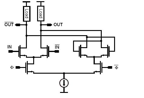
I am trying to design a CML/SCL latch. If I want a 700mv output swing, I assumed that the common mode input range of the latch for "IN" is atleast from VDD to 'VDD-0.7V'. The reasoning behind my assumption is that I will use the latch to form a Flip-Flop and a divider which requires the out_bar to connect to DIN. What should the common mode range of the CLK be? I am using biased current sources(pmos devices) as load devices.

How do I simulate the differential gain of this circuit in hspice? and how do I go about calculating the device sizes for this circuit?

Your comments are much appreciated!

52_1172713987.JPG
 

cml latch edaboard

High side of the clk/clkb can go up to Vdd, but you want to make sure your over drive (Vgs - Vt) isn't too high because then you may be in the region where the Ft & gm starts to drop off. So high side is determined at the voltage (Vgs - Vt) where Ft and gm starts to drop off or the value you can withstand. Your lowest level is determined by the resultant voltage on the clk/clkb transistor's source coupled node that will change the current of your current source. For example, if the voltage of the clk/clkb source coupled node is too low, your current source transistor (nmos) will no longer be in saturation. So that voltage will be determined by the VDSsat of your current source transistor or the resistor drop required for the current you need (if using a passive current source).

To get an estimation of gain, disconnect the cross-coupled latch transistors and calculate/simulate the gain of the diff pair.

For device size, your output pole is determined by 1/(2*pi*R*C). R is your load resistor, which is calculated by your swing divided by gate current. The C will be contribution of your Cgd of all transistors connected to that output plus the input capacitance of the next stage. You can optimize it to the bandwidth you are designing to. Once you know the current, look at the Ft vs. Id curves and pick a transistor whose Ft peaks at your gate current. You will probably have to optimized for your input pole later, if needed.
 
cml latch design

hi

you can use any common mode for clk provided the clk swing is capable of completely switching the mos on or off. i have designed latches in which the clk mos are either in triode or cut-off, but never in saturation. but i guess u need to have your input mos pair in saturation.

a common unintelligent way to size the mos is by choosing some initial sizes of the mos and keep increasing the size (and ofcourse the current) to get the latch to latch-up within a single clock cycle.
 

Status
Not open for further replies.

Part and Inventory Search

Welcome to EDABoard.com

Sponsor

Back
Top