Continue to Site

Welcome to EDAboard.com

Welcome to our site! EDAboard.com is an international Electronics Discussion Forum focused on EDA software, circuits, schematics, books, theory, papers, asic, pld, 8051, DSP, Network, RF, Analog Design, PCB, Service Manuals... and a whole lot more! To participate you need to register. Registration is free. Click here to register now.

what is the function for this resistor?

Status
Not open for further replies.

chang830

Full Member level 5
Joined
Feb 11, 2006
Messages
267
Helped
14
Reputation
28
Reaction score
3
Trophy points
1,298
Activity points
3,424
Hi,
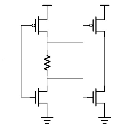
I have a question on the attached cicruit.

PLs. take a look at it. It is a simple inveretr at the output, the resistor in the circuit puzzled me. Would anyone can see what's the function of this resistor?

Is it for ESD function?

Thanks
 

did a simulation, can't see much difference it makes.
 

It is an iverter with fast rise time and slower fall time at the output. Since it is CMOS assuming it drives a CMOS load which presents a capacitive load, p-ch pulls up output fast but n-ch has extra resistor on top of its Ron so pulls down slower.
Another feature of this circuit is that, crowbar current reduced since during transition between Vdd and GND there is an extra resistor.

I hope it is clear.

Tekno1
 

    chang830

    Points: 2
    Helpful Answer Positive Rating
can you provide a SPICE testbench to see how it works? Thanks!
 

This will definitely help you as far as ESD. But it depends on the value of the resistor. For MM ESD it probably helps the NMOS if the resistor is of small value. For HBM ESD, I think this has to be like 1kOhm for it to significantly help ESD.
 

    chang830

    Points: 2
    Helpful Answer Positive Rating
It will increases the vol voltage of the circuit .
 

tekno1 said:
It is an iverter with fast rise time and slower fall time at the output. Since it is CMOS assuming it drives a CMOS load which presents a capacitive load, p-ch pulls up output fast but n-ch has extra resistor on top of its Ron so pulls down slower.

Agree.

tekno1 said:
Another feature of this circuit is that, crowbar current reduced since during transition between Vdd and GND there is an extra resistor.

True, and if you take outputs from both sides of the resistor, you have a simple non-overlapping driver to the next stage, which limit the shot through power loss.

44_1168488871.jpg

[/img]
 

    chang830

    Points: 2
    Helpful Answer Positive Rating
As ycj said, it's as non-overlaping ckt to limit the shoot-through current.
 

and if it is used as output buffer, then the resistor can improve the output impedance linearity with Vout, reduce reflection, and increase signal quality.
 

I think in the first place we should know is where the ckt is using.
 

Short circuiting the output to VCC will kill the NMOS if this resistor is missing.
This is a push-pull stage with "open drain feature". Designed for inequal sourcing and sinking currents.
 

Status
Not open for further replies.

Part and Inventory Search

Welcome to EDABoard.com

Sponsor

Back
Top