Continue to Site

Welcome to EDAboard.com

Welcome to our site! EDAboard.com is an international Electronics Discussion Forum focused on EDA software, circuits, schematics, books, theory, papers, asic, pld, 8051, DSP, Network, RF, Analog Design, PCB, Service Manuals... and a whole lot more! To participate you need to register. Registration is free. Click here to register now.

FTDI or Cypress chips???

Status
Not open for further replies.

STU_KNTU

Member level 1
Joined
Feb 29, 2016
Messages
33
Helped
3
Reputation
6
Reaction score
3
Trophy points
8
Activity points
286
Hi every one.
I want to transmit data with USB2.0 in some project's So i have to use a chip to handle physical layer and ... .

In your experience what company chips are better?
FTDI chips or Cypress Chips???
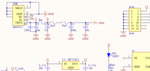
I have used FT245RL in Some project but honestly i was not satisfied from that chip for some reason.
In my project i want to configure my FPGA with the chip i will choose and i want to have hi speed communication too.

also may be i want to transmit data in super speed mode(USB3.0) in future.(sorry about the grammar :-|) and i want to focus in one of this companies chips...:thumbsup:


regards
 

Hi,

I use the FTDI chips but I don´t have experience with the Cypress chips, therefore I can´t say which one is better.

I have used FT245RL in some project but honestly i was not satisfied from that chip for some reason.
I´m surprised, because I´m very happy with them.

May I ask why especially you are not satisfied?
I find them easy to use. They operate very stable. And the throughput is more than 300kbytes/s. I find this OK for a USB1.1 type, which the FT245RL is.

But they have USB 2.0 bridge devices also. We achieved 25MBytes/s with a FT2232H.

Klaus
 
Cypress USB interfaces are quite good if you want to utilize HS or SS USB nearly up to the limit. Firmware overhead is considerably larger than with simple FTDI parallel FIFO chips.

If you want Superspeed with simple interface and configuration, the new FTDI FT600 series might be interesting.
 
thanks for you time.
in my view having enough examples and resource's,easy programming FPGA and low cost are my priorities to select the desired chip.

But they have USB 2.0 bridge devices also. We achieved 25MBytes/s with a FT2232H
your transmittance speed is quite well but i want to achieve almost 50Mbyte/s.

May I ask why especially you are not satisfied?
I had some problems in powering up and exchanging data.
For example in sending data to PC i always receive some constant numbers which i didn't send.
The schematic was the same as datasheet's schematic but when i connect the USB, PC didn't recognize the FTDI chip and i had to reset the FT245 with FPGA manually(power up issue ,i think :lol:)
i have started reading some cypress application note i have to say it has very comprehensive application note and datasheet...
 
Hi,

50Mbytes/s....I don't know if this is possible with USB2.0. It's close to the limit. For sure not with an FT245RL...

******

Honestly, I never experienced the problems you tell.
How was your power setup? Bus powered, self powered, or mixed?

You can show me/us your schematic and pcb layout....
Are your FTDI chips from a reliable source? There are fake copies around...

Klaus
 
I also have good things to say about FTDI and their drivers and their software support.

Some years ago I wrote a C# app that used their lower level driver to toggle the pins as I/O's and it all worked very smoothly. So did the normal serial use-case. We've also used them to drive a JTAG interface and have a plan to do that again on a larger scale.

Though I understand my company has used cypress too without any problems that I've heard about.
 
Honestly, I never experienced the problems you tell.
my be i was wrong....
however this is my schematic :
Captured.PNG
and my pcb layout with and without polygon
Capturedd.PNGCapturesss.PNG
it will be really helpful if you tell me what i was wrong :)
I also have good things to say about FTDI and their drivers and their software support.
what about my Priorities?
for example configuring FPGA and ....
 
Hi,

some issues:
* In the schematic the TEST pin is unconnected. It must be connected to GND. (I see in the PCB it seems to be connected. Why the discrepancy?)
* Why did you use two 47pF cpacitors at the USB line? I don´t think this makes sense. I assume the wires are terminated in the IC, then the Cs make things worse.
* A 100nF capacitor at RESET. To prevent from noise? I expect debouncing is done in th IC.
* you used 47k instead of 4k7 at the RESET input. Fur sure this may cause problems.
* mixed powering. Here I expect problems. It seems you have 5V external power supply wich via voltage regulator supplies VCCIO, but VCC is powered from USB.
Datasheets clearly says:
It should be noted that in this case this supply should originate from the same source as the supply to Vcc. This means that in bus powered designs a regulator which is supplied by the 5V on the USB bus should be used.
(I recommend do use a double schottky diode (BAT54C) to power VCC (one anode to USB_VCC, the other to SYSTEM_5V). Don´t forget the Cs.
* At VCC you have 100nF only, but datasheet shows 4u7 + 2 x 100nF
* You don´t use the recommended ferrite bead at VCC
* The resistor at PWREN is useless, but it will cause no problem.


****
Additionally I´m not a friend of the copper pour GND at the top side. This pretends to be a solid, stable GND signal, but it isn´t much better than wires. A true GND plane without splits is way better, use short traces from IC pin then a via to GND.
In your case some signal return paths through GND are long, complex and will have relatively high impedance. Especially the grounding of CDM_capacitor, PIN18, CDP_capacitor is really bad. Instead of filtering the USBDM signal you introduce the noise into the GND PIN18. They three need independent vias to GND. Urgent.

I hope you don´t mind my hard words, but the issues really may cause the problems you describe. Independent of FTDI or Cypress...

Klaus
 
thanks my friend ...

In the schematic the TEST pin is unconnected. It must be connected to GND. (I see in the PCB it seems to be connected. Why the discrepancy?)
it's unconnected in PCB too.the pin you have seen is AGND P25! my mistake...:thumbsdown:

* Why did you use two 47pF cpacitors at the USB line? I don´t think this makes sense. I assume the wires are terminated in the IC, then the Cs make things worse.
I have derived using this cap from FTDI app note's for edge control ...
based on this :
Captureddd.PNG
So are you saying i shouldn't use this cap's?
* A 100nF capacitor at RESET. To prevent from noise? I expect debouncing is done in th IC.
yes, but i don't think this make any problem.is this?!
you used 47k instead of 4k7 at the RESET input. Fur sure this may cause problems.
No.that was my mistake in schematic.in PCB i used 4.7k resistor.
mixed powering. Here I expect problems. It seems you have 5V external power supply wich via voltage regulator supplies VCCIO, but VCC is powered from USB.
No.i have used VUSB alone.
difference between 5vusb and 5v is that there is a ferrite bead between them .

At VCC you have 100nF only, but datasheet shows 4u7 + 2 x 100nF
* You don´t use the recommended ferrite bead at VCC
I have used alot capacitor for 5vusb based on my circuit.
but they not very close to chip.
the actual power circuit is this :
dd.PNG
the fer2 in nothing.!! the fer1 and fer is ferrite bead. i have used fre1 for some reason that is not concern with usb chip.
As you see i have used 4.7u and other caps as FTDI's app note.
i have used 220u cap arbitrary! it doesn't change any difference in FTDI's chip working because i used that when i was delivering my project!

Additionally I´m not a friend of the copper pour GND at the top side. This pretends to be a solid, stable GND signal, but it isn´t much better than wires. A true GND plane without splits is way better, use short traces from IC pin then a via to GND.
In your case some signal return paths through GND are long, complex and will have relatively high impedance. Especially the grounding of CDM_capacitor, PIN18, CDP_capacitor is really bad. Instead of filtering the USBDM signal you introduce the noise into the GND PIN18. They three need independent vias to GND. Urgent.
can you explain me more?!
i under stand what are you saying but i think my PCB is okay! most probably i am wrong but i don't know where...
 

Attachments

  • dd.PNG
    dd.PNG
    31.1 KB · Views: 101
Last edited:

Hi,

TEST pin: urgent!

47pF: If you don´t have problems, then don´t change it. In case of errors you may try without them.

100nF @ RESET: It depends on the FTDI internal circuit. In doubt, or problems, keep on the FTDI datasheet and don´t use the capacitor.

Mixed powering: You say your system is bus powered only. Here again: In doubt, or problems, keep on the FTDI datasheet.
Check the datasheet:
* USB_VCC from the plug is only connected to a 100nF capacitor and the ferrite bead. noting else. But you use 220uF (I´m not sure if this is allowed by USB_specification)
* After the bead .. it is used for powering the FTDI and your application.
* Definitive OFF USB_specification is the direct powering of your application from the USB_supply. You need to use the switch. During power up and USB_device initialisation there is only a limited current draw allowed. The USB_host (PC) decides if the application may draw more power or not (PWREN signal). I know many devices violate the specification in this, but in case of problems don´t blame it on FTDI, USB, Cypress, or someone else. Usually the PC doesn´t switch USB_power, it has to be done by the USB_device.

Generally: adding inductance may be critical. They for a resonance with the surrounding capacitors. The oscillation must be damped. Either the bead itself or the load does this. If not you need to install a damping circuit. Especially your L-C-L combination is critical.

Layout:
Imagine a transient EM pulse on the USB_DM_line. Folow it´s current:
USB-plug --> USB_DM capacitor --> capacitor GND pad --> thin wire --> FTDI_GND pin 18 (now you feed the pulse to the FTDI instead of attenuate the pulse) --> thin wire --> 3V3 capacitor (now you feed the pulse to the FTDI3V3) --> thin wire --> USB_DP capacitor --> USB_plug_GND --> finally it reaches the via to solid GND plane.

I modified your layout.
Grey: deleted traces
Green: my changes
FTDI1.PNG

Klaus
 

I modified your layout.
Grey: deleted traces
Green: my changes
you're right.
certainly this is better.
but still my question doesn't answered...
So are you saying FTDI's Chip can support all my needs based on what i mentioned below and hi speed transfer rate too?
in my view having enough examples and resource's,easy programming FPGA and low cost are my priorities to select the desired chip.
 

Nice posting by Klaus.


Yes when I said JTAG I meant in the context of FPGA configuration.

Which FPGA's are you using? Both Xilinx and Lattice programming tools either support or can be tricked into supporting an on-board FTDI chip natively (no experience with Altera). That is the lattice programming tool treats your on-board FTDI chip just as it would their programming dongle (because their dongle presumably just has an FTDI chip inside). Lattice dev boards use this method and you can copy their schematics.

Xilinx seems a bit more coy, some of their dev boards embed an FTDI chip for programming but they don't seem to openly support or encourage it. Though you can find people online who get Xilinx tools to support their FTDI chip if its configuration EEPROM has the right values (repeating what a colleague told me here).

Whatever chip you're configuring make sure to look for existing support. And regardless when I say FTDI has good support what I mean is that they specifically provide examples for implementing generic JTAG, SPI or I2C interfaces. So they're well suited for FPGA configuration of any kind.
 

Status
Not open for further replies.

Part and Inventory Search

Welcome to EDABoard.com

Sponsor

Back
Top