Continue to Site

Welcome to EDAboard.com

Welcome to our site! EDAboard.com is an international Electronics Discussion Forum focused on EDA software, circuits, schematics, books, theory, papers, asic, pld, 8051, DSP, Network, RF, Analog Design, PCB, Service Manuals... and a whole lot more! To participate you need to register. Registration is free. Click here to register now.

[SOLVED] OTA Folded Cascade design procedure

Status
Not open for further replies.

gianni66

Junior Member level 3
Joined
Jan 26, 2016
Messages
31
Helped
0
Reputation
0
Reaction score
0
Trophy points
6
Activity points
251
Hi everyone,
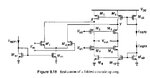
I need to design and validate a Folded Cascade OTA for University, but I don't really know where to start from, since I've not been given particular specs.
I wonder how the process is in such cases, for example if I have to decide (reasonably) some specs and then extrapolate the others, or proceeding in a different way.
I would be glad if someone could suggest some books/reads who can drive me through this.
 

Re: OTA Folded Cascode design procedure

Check the Similar Threads below.
 
Re: OTA Folded Cascode design procedure

CMOS Circuit Design Layout and Simulation for R. Jacob Baker and

CMOS Analog Circuit Design for Allen Holberg

These good book if you are looking for a design.
 
Re: OTA Folded Cascode design procedure

Thank you for the tips. I've checked out your books and they turned out useful, but I need some more advice.
I attach the topology I should follow, taken from Razavi's book. It is explained and an example is given but, sorry about the question, I don't understand what I should put in practice where there are Iref1, 2 and 3, as the circuit is "cut".
 

Attachments

  • OTAFOLDED.jpg
    OTAFOLDED.jpg
    52.4 KB · Views: 129

Re: OTA Folded Cascode design procedure

... I don't understand what I should put in practice where there are Iref1, 2 and 3, as the circuit is "cut".

Just read on the following 2 pages with the Example 9.6 and its Solution.
 

Thanks for your answer erikl, and sorry for the "stupid" question (I've studied a lot of electronics in theory, but I've never done an analog design like this). Anyways, I had already checked out that example but it looks a little too hard to understand for now in some points. I'll study more and ask again if I have problems.
 

Hi, I have been busy with other projects recently and now I'm back to business.
Thanks to you advice (and especially to Razavi and Allen's books) I think I'm ready to do it, but still I have a problem: my professor gave us Level 7 MOS models which include their parameters BUT there's no mention about channel length modulation effects.
So my question is: I have to determine ro for every transistor to compute the stage gain the analytic way, but I don't know my lambda (and so I don't know the devices' VA). Is there any alternative way to do it, without such parameter? The only possible "solution" I have came up with is to simulate MOS' characteristics and then, by using two points on the graph, to compute VA, but I doesn't seem like a feasible (accurate) solution to me.
 

I have to determine ro for every transistor to compute the stage gain the analytic way, but I don't know my lambda (and so I don't know the devices' VA). Is there any alternative way to do it, without such parameter? The only possible "solution" I have came up with is to simulate MOS' characteristics and then, by using two points on the graph, to compute VA, but I doesn't seem like a feasible (accurate) solution to me.

The slope of the Id vs. Vds characteristic gds, respectively the inverse of ro = VA/Id depends on the operation point (OP), at least so long as it isn't far out at the Id-vs-Vds curve (where gds stays rather constant). So if you have to follow this calculation method, I think it's the best to use ro = 1/gds directly from the intended OP from your simulation result.
 
I do not have to follow any particular procedure, but I obviously have to justify my design and, most importantly, I want to understand everything i do, that's why I asked if there is any alternative way to define ro.
All of the designs I have checked so far (from Sedra-Smith, Allen's book, Razavi's book) use that kind of procedure and start with fixed values for N and P devices which looked a bit odd to me, don't know if it is an approximation.
 

Ok, tried to do what I intended to do and honestly I don't like it very much. Any procedure suggested?
 

I'm sorry for triple posting, but I found in older posts that I could be proceeding in this way:

-Finding LAMBDA (or VA) for a certain graph (e.g. minimum channel length) and obtain a VA' value dividing for the min channel length
-Extend that rule in case i use a different value of channel length, using a relation like VA = VA' * L
 

Please have a look into P.E. Allens Slides: **broken link removed**
Here the design procedure is explainend in very detail. As erikl mentioned you should get your gds within your OP. Just do a DC analysis where the output of your AMP is connected to the input (follower). Afterwards you can go on with your AC analysis within this OP (cut the connection between output and input - sp2tswitch). A good starting point for your Ls is 3-5x Lmin. Please note increasing L makes your circuitry slower but also increases gds and therefore the intrinsic gains. Having said this you should also consider that increasing the area of a MOSFET increases the prasitic capacity and therefore the poles are shifted to a lower frequencies.

Have fun ;)

BR
Lukas

Edit: Use one ideal current source for your design. you can generate the other reference currents by using current mirrors. Concerning your question: At the bottom of the cut branches you need a NMOS that is part of a current mirror. The diode connected PMOS transistors are used to generate the biasing voltage for the folded cascode (principle of current mirror).
 
Last edited:
Thanks a lot for your answer, it helped. I'm gonna check that out in the next days and give feedback!
 

Ok, I've seen his analysis and I've understood a lot from it. So, I should start my design using 3-5x Lmin, follow his procedure to determine all the aspect ratios for the transistors and then perform a DC analysis getting gds' value to calculate the differential voltage gain?
 

Yes.. Do the DC analysis (connected as follower) with your initial W/L ratios then you can go on with the AC analysis (open loop - cut the connection by using the sp2tswitch; it applies different switch positions for different type of analysis). If you change any dimension you have to repeat the DC to get the proper OP for your AC analysis. For AC analysis your circuit gets linearised in the OP that is provided by the DC analysis. Use a small input amplitude for your AC analysis (VAC).
Just an example: If your gain is to low increase L at the output stage to get higher output resistance. BUT more length also means slower circuitry as the area and therefore the capacitance is increased. Take care and invest some time.. you will understand how it works ;)

BR Lukas
 
Hi, thank you for your answer.
I went on and I'm gonna attach the biased circuit here. I started giving some specs which were:
-SR = 10 V/us (I checked out other OTA projects and this parameter is usually higher)
-CL = 10 pF (As mentioned above, this might be too big)
-Max/Min Output Level -> 2.5 V, 0.5 V
-GBW = 10 MHz
-Input Common Mode Max/Min = 1 V, 2.5 V
-Gain > 5000

Using these constraints i dimensioned my transistors, I would like to know which of them look reasonable. I followed your suggestion and decided to use 5x Lmin to be sure to reach the required gain but with hand calculations it is approximatively 8500 which is a lot higher, and it is even higher in simulation. I think i would re-make the project using a smaller CL, higher SR and maybe higher GBW (depends on CL tho). I simulated Bode diagrams for amplitude and phase, and of course I know I can measure phase margin for example. Would it be useful to make other simulations?
OTAFREQ.PNG
OTABIAS.PNG
 

M11 might be the problem: Not saturated I guess. Please check your DC levels. Look at the Gate of M7,M8 -> xxx nV
 
You're absolutely right. Gonna figure it out
 

I checked back the project in Cadence and that voltage is 0.7 V, which is correct (I mean M7, M8), and M11 should be saturated swell since VDS = 0,269 > VGS - VTh = 0,724 - 0,498 = 0,226. Correct me if I'm missing something
 
Last edited:

I have re-made my project and it works fine (hand calculated specs meet quite accurately simulated specs). Now I'm writing a small relation about my work. Which simulations would be useful to insert? For now, I simulated bias points using DC analysis, frequency and phase diagrams using AC sweep. I would like to simulate a step to see if the slew rate spec is ok. Does it have any sense to do so? How could I proceed? Short in-out?
 

Status
Not open for further replies.

Similar threads

Part and Inventory Search

Welcome to EDABoard.com

Sponsor

Back
Top