anhnha
Full Member level 6
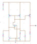
I am designing an op-amp based bandgap reference and getting this problem.
**broken link removed**
**broken link removed**
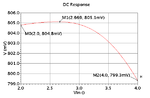
As Vdd increases, the output of op-amp also increases but at a much higher rate=> Vsg of M11, M12 decrease and the currents flowing through these transistors decrease=> bandgap voltage decreases.
Could anyone tell me how to solve this?
**broken link removed**
**broken link removed**
As Vdd increases, the output of op-amp also increases but at a much higher rate=> Vsg of M11, M12 decrease and the currents flowing through these transistors decrease=> bandgap voltage decreases.
Could anyone tell me how to solve this?
")