yupina-chan
Member level 2
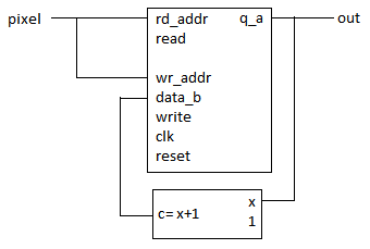
hi. i have a histogram module which worked fine when simulated. now, i want to apply it in image processing. i use terasic d5m camera and after taking a snapshot, i would like to take its histogram. i have read that a ram block is needed to implement it to fpga. what i don't understand is how to do it. can you give me hints in doing this? or a diagram on input and output ports of the histogram and ram block. thanks in advance.
i have included my histogram code. will this be okay for my desired implementation?
i have included my histogram code. will this be okay for my desired implementation?
Code:
module histogram(data_in, out1, out2, out3, out4, out5,out6,out7,out8, clk, reset);
output reg [7:0] out1;
output reg [7:0] out2;
output reg [7:0] out3;
output reg [7:0] out4;
output reg [7:0] out5;
output reg [7:0] out6;
output reg [7:0] out7;
output reg [7:0] out8;
input [7:0] data_in;
input clk;
input reset;

always @ (posedge clk or negedge reset)
	begin
	if (!reset)
	begin
			out1 <= 0;
			out2 <= 0;
			out3 <= 0;
			out4 <= 0;
			out5 <= 0;
			out6 <= 0;
			out7 <= 0;
			out8 <= 0;
	end
	else
	begin
			if (data_in >= 8'b11100000)
			begin
				out8 = out8 + 1;
			end
			else if (data_in >= 8'b11000000)
			begin
				out7 = out7 + 1;
			end
			else if (data_in >= 8'b10100000)
			begin
				out6 = out6 + 1;
			end
			else if (data_in >= 8'b10000000)
			begin
				out5 = out5 + 1;
			end
			else if (data_in >= 8'b01100000)
			begin
				out4 = out4 + 1;
			end
			else if (data_in >= 8'b01000000)
			begin
				out3 = out3 + 1;
			end
			else if (data_in >= 8'b00100000)
			begin
				out2 = out2 + 1;
			end
			else if (data_in >= 8'b00000000)
			begin
				out1 = out1 + 1;
			end
	end
	end

endmodule
") --- A(n+1) .....
--- A(n+1) .....