Continue to Site

Welcome to EDAboard.com

Welcome to our site! EDAboard.com is an international Electronics Discussion Forum focused on EDA software, circuits, schematics, books, theory, papers, asic, pld, 8051, DSP, Network, RF, Analog Design, PCB, Service Manuals... and a whole lot more! To participate you need to register. Registration is free. Click here to register now.

[VHDL] How to change signal logic

Status
Not open for further replies.

spade7

Newbie level 5
Joined
Jan 27, 2013
Messages
8
Helped
0
Reputation
0
Reaction score
0
Trophy points
1,281
Activity points
1,356
Hello,
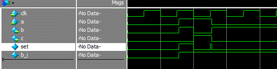
I am rather new on VHDL. I have done some code in the past but I have a problem concerning how to manipulate B and C signals (as shown below). Actually, it is a state machine and I am trying to change the logic of these signals (B & C) in half of the clock pulse. Could you please give me some hints how to do it? Thank you


clocksignals.jpg
 

it would be quite easy to do with VHDL, but impossible on an FPGA.

Just double your clock speed and its all possible.
 

it would be quite easy to do with VHDL, but impossible on an FPGA.

Just double your clock speed and its all possible.


Do you mean to have a second clock for the signals B & C which runs on double speed of the global clock? This is Implemented on FPGA . Am I correct?
 

no, just have your global clock run at double speed.
 

no, just have your global clock run at double speed.

Tricky thank you very much . I cannot change the speed of the clock. But in any case even if I change the speed of the clock the signals B & C will change in a clock cycle (full) and not as the diagram shows (half cycle).
 

if you cannot change to a 2x clock, then it will be impossible to implement B and C.
 

Since each state takes one clock cycle Even if I x2 the clock speed then the state will change in one clock cycle but faster. Sorry but I cannot understand what will be the difference. The waveform states that B & C change logic in half clock cycle not in a full clock cycle.
 

At double the clock speed, A is high for two clock cycles and B and C are each pulsed for one clock.

You would rewrite your logic accordingly.


r.b.
 

if you cannot change to a 2x clock, then it will be impossible to implement B and C.

Given the challenge of it's impossible.... ;-)

Here is a Verilog solution as I don't use VHDL regularly.

Code Verilog - [expand]
1
2
3
4
5
6
7
8
9
10
11
12
13
14
15
16
17
18
19
20
21
22
23
24
25
26
27
28
29
30
31
module fukdup (
  input      clk,
  input      a,
  output     b,
  output reg c
);
 
reg set = 1'b0;
reg b_i = 1'b0;
 
always @ (negedge clk or negedge a) begin
  if (!a) begin
    c <= 1'b0;
  end else begin
    c <= a;
  end
end
 
always @ * begin
  set = a & clk;
end
 
always @ (posedge set) begin
  if (set) begin
    b_i <= 1'b1;
  end
end
 
assign b = b_i & ~c;
 
endmodule


Of course I would never use code like this unless my back was to the wall and my boss put a gun to my head. ;-)
 

Thank you all very much for the help!:)
 

Thank you all very much for the help!:)

I bet this was a homework problem...I also bet you haven't learned a thing from my post.

It took me about 10 minutes to design and simulate this code. The objective of this assignment was probably to get you to think creatively and come up with a solution without resorting to doubling the clock frequency. The code I posted would be considered a band-aid (rightly so) and wouldn't be fit for use in any product that a customer would buy. I would first generate a 2x clock in the FPGA I was using and eat up another clock domain just for these two signals before resorting to such a band-aid solution.

If I had to resort to such a band-aid, I would hand place each cell and run the design over temp/voltage variations to ensure whatever is using those half clock cycle pulses will work reliably.

Oh, well, you probably don't even realize that I did you a disservice by posting the code, you're probably just happy you'll get a good grade by using someone else's design.


I have checked your code but I am still doing the code with x2 clock to check if it behaves accordingly. checking every possible implementation once a time :) This was just a small part off all the signals I have to implement under this status , so it is taking tame.I have not reject reading and analyzing your code. I have tried different thinks for example passing through an AND gate Clk and A signal in order to produce B. another was to use DFF e.t.c I feel really grateful for what you have write and i will come up with the results. However, I think that this is offensive by telling me "you're probably just happy you'll get a good grade by using someone else's design".
 

However, I think that this is offensive by telling me "you're probably just happy you'll get a good grade by using someone else's design".

Sorry about that, I apologize. :oops: I now see you are actually willing to do your own work and experiment with different solutions. I've become rather cynical in the short time I've been using this forum as many of the posters aren't willing to try anything before posting. They just want the answers handed to them. I'm glad to see your not one of them.

I still feel the solution I proposed along with your gated clock solution are band-aids and should be avoided at all cost.

Watch out with the gated clock solution as you'll have to account for the delays through the LUTs resulting in many glitches in the output signals. I once had the misfortune of having to "fix" a gated clock design in an FPGA done by another engineer. Took months to fix the 100's of gated clocks, which I had to hand place and hand route to meet timing and remove glitches. That was the last time I let a manager tell me to just fix the design because it's almost working. Next time I had to work on another broken design, from that engineer, I threw the design away and started from scratch.
 

    spade7

    Points: 0
    No comments
Thank you but you don't have to apologize. I might misunderstood your sayings as well. :) I always want to experiment and select which seems to be the best for each situation. That's why I have asked for Hints.

Yes, I agree about the gated-clock. I have done asynchronous alot in the past and have used it in GALS at some point but they are tricky to start experiment with them as well. However power is not something concerns me at this project.

It is really good that you had referred to the gated-clock and how dangerous is to do it! Everybody should know that these tricks can put you in trouble. keep the things simple.!:)

Actually, I am trying the x2 clock. I have seen that everybody agrees here! Based on the waveform I have uploaded I am using his clock to feed the next Entity and for controlling the other signals (A.B.C) I had made another clock double the period that "stays" only on this Entity. Haven't written VHDL for almost 5 years it makes me a bit slow!

I will come up with the results! That will be my thanks to you guys!:)
 
Last edited:

if you cannot change to a 2x clock, then it will be impossible to implement B and C.

Its entirely possible with 1x clock, but device dependent. Chances are favorable that the FPGA has DDR registers in it.

Xilinx example:
1. Instantiate an ODDR primitive (or ALTDDIO_OUT for Altera).
2. To create 'B', tie: 'CLK' to clock input, CE (Clock Enable) to 'A' or '1', D1 (data on rising edge) to '1', D2 (data on falling edge) to '0'. Where 'A' goes and what CE does will depend on your design.
3. To create 'C', reverse your D1 and D2 lines but keep everything else the same. (So D1 = '0' and D2 = '1'). Gate the Q output with 'A' (for Altera see note below).
Done.

See ODDR
https://www.xilinx.com/support/documentation/user_guides/ug361.pdf

Here's the Altera literature in case anyone else is wondering, see 3-20.
https://www.altera.com/literature/ug/ug_altddio.pdf
Note: For this primitive you would tie the 'A' line to OE (output enable). This will result in a high 'Z' at the pad however.

Again, this solution is device dependent and you might have to play around with pieces of the IOB in order to gate the output signal of the DDR register properly (before going to the pad). You might also have to run 'A' to the clock enable of the DDR register as well. The solution depends a lot on your design and what you're trying to do with these signals.
 
Last edited:

BlackHelicopter,

My version doesn't require DDR I/O registers, which spade7 doesn't seem to want based on his using the outputs b and c in another module. Besides my code does synthesize in Xilinx and I'm sure it will in Altera too (though I'm not going to bother trying). Pretty much any FPGA/ASIC device should support it as long as it supports a falling edge clock.

Of course I don't recommend using it as it's just a band-aid, but it does result in outputting the waveforms for b and c without glitches. Though you could easily end up with much less than a half cycle transition if the cells are far apart, hence my recommendation to hand place the logic. It would also be a pain having to write the constraints for this circuit. ;-) note: I didn't write any when I tested it in the synth/placer/route tools.

I think spade7 is better off using the 2x clock version for just the small amount of logic that he needs and just make sure he doesn't cut timing between the two clock domains as they aren't asynchronous.
 

I agree with you, the 2x would be the best/easiest approach. :cool:

I was more or less making an attempt at trying to disprove of it being impossible (I can't resist a good challenge) :razz:
 

It wasn't impossible, I proved that...try running my code in a simulator. :)
 

I see what you're talking about now! I missed that part oops. :razz:
 

Here's a simulation run of it.


I scared myself when I shifted the a signal over to the falling edge, and it broke the simulation...that was the perfect example of why this type of circuit is highly dependent on delays and is a band-aid.
waveform_broken.GIF

See what delaying a does to the waveform :-(
 

Status
Not open for further replies.

Similar threads

Part and Inventory Search

Welcome to EDABoard.com

Sponsor

Back
Top